SLWS230E September 2011 – December 2015
PRODUCTION DATA.
- 1 Features
- 2 Applications
- 3 Description
- 4 Revision History
- 5 Pin Configuration and Functions
- 6 Specifications
- 7 Detailed Description
- 8 Application and Implementation
- 9 Power Supply Recommendations
- 10Layout
- 11Device and Documentation Support
- 12Mechanical, Packaging, and Orderable Information
5 Pin Configuration and Functions
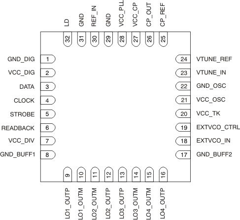
RHB Package
32-Pin VQFN
Top View

Pin Functions
| PIN | I/O | DESCRIPTION | |
|---|---|---|---|
| NO. | NAME | ||
| 4 | CLOCK | I | Serial programming interface, clock input |
| 26 | CP_OUT | O | Charge pump output |
| 25 | CP_REF | — | Charge pump reference ground |
| 3 | DATA | I | Serial programming interface, data input |
| 19 | EXTVCO_CTRL | O | Digital control to enable/disable external VCO |
| 18 | EXTVCO_IN | I | External VCO input |
| 29 | GND | — | Ground |
| 31 | GND | — | Ground |
| 8 | GND_BUFF1 | — | Output buffer ground |
| 17 | GND_BUFF2 | — | Output buffer ground |
| 1 | GND_DIG | — | Digital ground |
| 22 | GND_OSC | — | VCO core ground |
| 32 | LD | O | Lock detector output |
| 10 | LO1_OUTM | O | LO1 output: negative pin |
| 9 | LO1_OUTP | O | LO1 output: positive pin |
| 11 | LO2_OUTM | O | LO2 output: negative pin |
| 12 | LO2_OUTP | O | LO2 output: positive pin |
| 14 | LO3_OUTM | O | LO3 output: negative pin |
| 13 | LO3_OUTP | O | LO3 output: positive pin |
| 15 | LO4_OUTM | O | LO4 output: negative pin |
| 16 | LO4_OUTP | O | LO4 output: positive pin |
| 6 | READBACK | O | Serial programming interface, readback |
| 30 | REF_IN | I | Reference signal input |
| 5 | STROBE | I | Serial programming interface, latch enable |
| 27 | VCC_CP | — | Charge pump power supply |
| 2 | VCC_DIG | — | Digital power supply |
| 7 | VCC_DIV | — | Divider power supply |
| 21 | VCC_OSC | — | VCO core power supply |
| 28 | VCC_PLL | — | PLL power supply |
| 20 | VCC_TK | — | VCO LC tank power supply |
| 23 | VTUNE_IN | — | VCO control voltage |
| 24 | VTUNE_REF | — | VTUNE reference ground |