SLYA036B July 2018 – November 2021 DRV5053 , DRV5053-Q1 , DRV5055 , DRV5055-Q1 , DRV5056 , DRV5056-Q1 , DRV5057 , DRV5057-Q1
- Trademarks
- 1Introduction
- 2Overview
- 3Device Descriptions
-
4Methods
- 4.1 Uncalibrated Implementations
- 4.2 Peak Calibrated Implementations
- 4.3 Lookup Table Calibration Implementations
- 4.4 Peak Calibrated Plus Lookup Table Hybrid
- 5References
- 6Revision History
4.2.2.1 Specific Implementation
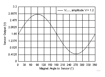
With one sensor, as in Figure 4-2, the sensor output voltage takes the form shown in Figure 4-10. With a peak calibration phase, both the min and max voltage values are known.
 Figure 4-10 One Sensor Peak Calibrated Data