SLYA042 July 2024 FDC1004 , FDC1004-Q1
- 1
- Abstract
- Trademarks
- 1 Introduction
- 2 CSAs and Input Bias Stage
- 3 CSA and Gain Error Factor
- 4 Applications for Resistance at Input Pins of Current Sense Amplifiers
- 5 Applications for Input Resistance at Reference Pins of Current Sense Amplifiers
- 6 Design Procedure and Error Calculation for External Input Resistance on CSA
- 7 Design Procedure for Input Resistance on Capacitively-Coupled Current Sense Amplifier
- 8 Design Procedure for Input Resistance at CSA Reference Pins
- 9 Input Resistance Error Test with INA185 Over Temperature
- 10Input Resistance Error Test with INA191 Over Temperature
- 11Derivation of VOS, EXT for a Single Stage Current Sense Amplifier (CSA)
- 12Summary
- 13References
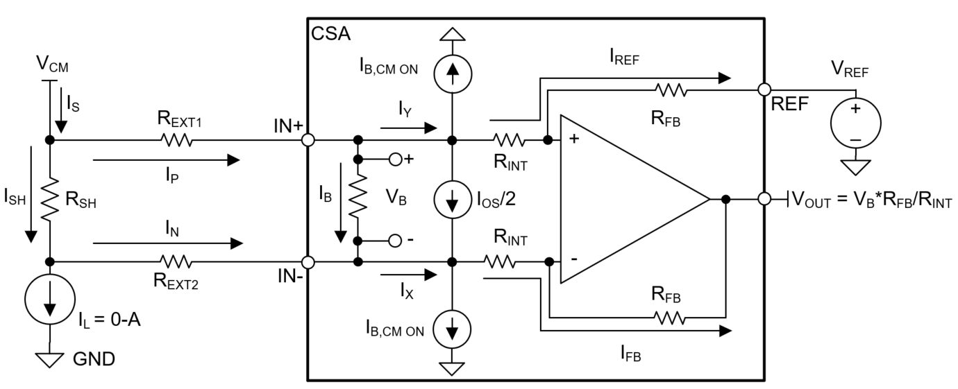
11 Derivation of VOS, EXT for a Single Stage Current Sense Amplifier (CSA)

This derivation assumes a single-stage, linear CSA. Derivation first begins by determining VB (bias voltage across bias resistor) when load (IL) is 0A as this is essentially VOS, EXT RTI. Then this is divided by gain error factor (GEF) to get the referred-to-shunt offset error (VOS, EXT RTS). Note that this derivation also requires a more specific equation for GEF which assumes that the REXT value at each pin can be different.
(4) into (3) and (5) into (2)
(2) into (7)
(7) into (8)
(1), (3), and (9) into (6).
(8) into (6). Solve for VB
Determine Gain Error Factor when REXT1 does not equal REXT2. You can simply remove ICM, ON, IOS sources, and set VCM and VREF sources to 0V as these only affect the offset. Gain is constant throughout operational VCM.
(5) into (2)
(2) into (7)
(2), (8) into (10).
(7) into (10). Solve for VB/VSH = GEF