SLYA042 July 2024 FDC1004 , FDC1004-Q1
- 1
- Abstract
- Trademarks
- 1 Introduction
- 2 CSAs and Input Bias Stage
- 3 CSA and Gain Error Factor
- 4 Applications for Resistance at Input Pins of Current Sense Amplifiers
- 5 Applications for Input Resistance at Reference Pins of Current Sense Amplifiers
- 6 Design Procedure and Error Calculation for External Input Resistance on CSA
- 7 Design Procedure for Input Resistance on Capacitively-Coupled Current Sense Amplifier
- 8 Design Procedure for Input Resistance at CSA Reference Pins
- 9 Input Resistance Error Test with INA185 Over Temperature
- 10Input Resistance Error Test with INA191 Over Temperature
- 11Derivation of VOS, EXT for a Single Stage Current Sense Amplifier (CSA)
- 12Summary
- 13References
1 Introduction
Most current sense amplifiers (CSA) have input resistances much lower than similarly closed-loop instrumentation (in-amps) and difference amplifiers. This is primarily because of the non-isolated connections to the inputs pin, but also due to the input bias stage in between input pins. Thus, CSAs ideally should have little to no external input resistances (REXT < 10Ω) at input pins; however, certain applications may require higher REXT and thus it becomes crucial to understand and calculate worst-case error to see if circuit still meet system requirements.
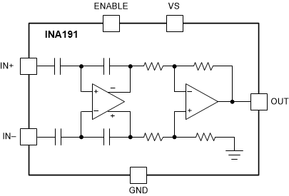
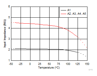
In recent years, capacitively-coupled input current sense amplifiers (for example, INA190 or INA191) can present much higher effective differential resistances in the range to 2MΩ to 5MΩ over temperature.
 Figure 1-1 Simplified INA191 Functional Block Diagram
 Figure 1-2 INA191 Differential Input Resistance Over Temperature
These devices can easily measure lower current in the micro-Amps range and also maintain high accuracy with larger input resistors. Note that capacitively-coupled input amplifiers often require some differential input capacitance at the input pins whenever significant external impedance is present. This is to help provide charge to internal switching capacitors.
The other important input loading resistance for most CSAs and difference amplifiers is the reference voltage source resistance (REXT3). Reference (REF) pins allow the output of bidirectional CSAs to be biased to voltage when the measuring 0-V differentially. System design cost and complexity can be reduced by simply driving REF pins with a resistor divider as opposed to a low-impedance source. However, all error sources and loss of dynamic range must be considered and bounded. For a detailed analysis of error generated from loading REF pins, refer to Driving Voltage Reference Pins of Current-Sensing Amplifiers, application note.
Overall, higher input impedance devices can be more accurate with external loading; however with only a few specifications of process variation, a system designer using a CSA with REXT >10Ω can achieve manageable error targets in low-accuracy, but low-cost and small PCB systems. This document shows how to calculate the bounds of this input resistance over temperature. In many cases a one-point, offset calibration is most practical.