SLYA042 July 2024 FDC1004 , FDC1004-Q1
- 1
- Abstract
- Trademarks
- 1 Introduction
- 2 CSAs and Input Bias Stage
- 3 CSA and Gain Error Factor
- 4 Applications for Resistance at Input Pins of Current Sense Amplifiers
- 5 Applications for Input Resistance at Reference Pins of Current Sense Amplifiers
- 6 Design Procedure and Error Calculation for External Input Resistance on CSA
- 7 Design Procedure for Input Resistance on Capacitively-Coupled Current Sense Amplifier
- 8 Design Procedure for Input Resistance at CSA Reference Pins
- 9 Input Resistance Error Test with INA185 Over Temperature
- 10Input Resistance Error Test with INA191 Over Temperature
- 11Derivation of VOS, EXT for a Single Stage Current Sense Amplifier (CSA)
- 12Summary
- 13References
6.1 Calculating eEXT for INA185A4 With 110Ω Input Resistors
Use the previous equations to perform an analysis on a hypothetical circuit with the INA185A4 with 110Ω resistors (REXT) at input pins. Consider the following circuit parameters:
| Parameter | Nominal Value | Tolerance | Drift (ppm/°C) |
|---|---|---|---|
| VS | 5V | 0% | 0 |
| VCM | 12V | 0% | 0 |
| TA, Max | 100°C | N/A | N/A |
| RSH | 1mΩ | 0.1% | ± 50ppm/°C |
| REXT | 110Ω | 0.1% | ± 20ppm/°C |
| RFB | 500kΩ | Process Variation (PV) ± 20% | Process Variation Temperature Coefficient = ± 30ppm/°C |
| RINT | 2.5kΩ | ||
| RBIAS | 2.5kΩ | ||
| IOS/2 Max | ± 225nA | 0 | ± 10 |
| IB, CM ON | 58µA | 20% | ± 157ppm/°C |
| GainDevice | 200V/V | 0.25% | ± 8ppm/°C |
| GainTotal, Typical | 176.67844523V/V | Variable | Variable |
Most of the fundamental circuit parameters needed are found in data sheet. However there is some calculation and estimation needed for IOS and IB, CM ON.
Typical IOS is usually very small; however, this can increase for any ratio mismatch between the RBIAS/2 resistors seen in Figure 2-1 and mismatch between the RINT and RFB resistors on the positive (non-inverting) and negative (inverting) branches of the internal amplifier network.
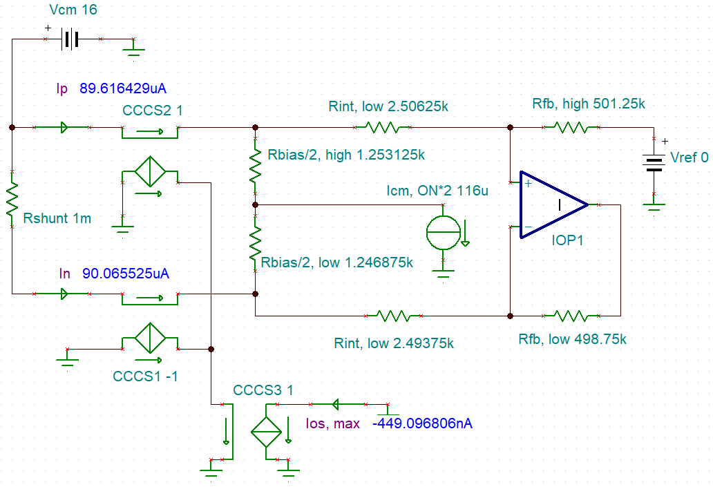
As stated previously, matching of resistors ratios is very small, but can be conservatively approximated by device's typical gain error of ±0.25%. Using this information, one can simulate the ideal amplifier network and measure maximum IOS by setting all resistors in one branch to +0.25% and in the other branch set to -0.25%. For VCM = 16V, IOS is 450µA. Since all resistors will have the same drift, IOS drift will be fairly low and simply approximated as 10ppm/°C. If a one-point calibration is performed, then error from IOS will be negated. Please contact TI support for more information if necessary.
 Figure 6-1 Worst-Case IOS For
Single-Stage CSA
Figure 6-1 Worst-Case IOS For
Single-Stage CSAFor IB, CM ON, the typical value is simply the jump in IB, CM as shown in Figure 2-2. Tolerance can be approximated as process variation. Drift can be deduced by IB, CM versus temperature data plots in data sheet. For the INA185, the data sheet shows a 2µA change in IB, CM from -40°C to 125°C. Assume this value is 3µA and you can determine drift in ppm/°C as:
Lastly temperature dependencies in VS and especially VCM need to be considered as these can add to the offset drift, which cannot be calibrated.
The calculated eEXT values at 25° and maximum ambient temperature are shown in Table 6-2.
Offset Values are Referred-to-Shunt (RTS) Using Worst-Case GEF at 125°C
| TA (°C) | High | Low | |
|---|---|---|---|
| VOS, EXT Max (µV) | 25 °C | 71.45 | -71.25 |
| 125 °C | 115.82 | -115.62 | |
| EG, EXT Max | 25 °C | 1.99209% | -2.84638% |
| 125 °C | 2.04245% | -2.91539% | |
| EG EXT, Drift (ppm/°C) | 5.057 | -6.902 | |
| VOS EXT, Drift (µV/°C) | 0.442 | -0.444 | |
| VOS, EXT Calibrated, 25°C (µV) | 44.37 | -44.37 | |
Note that worst-case VOS, EXT occurs when PV = -20%.
Table 6-3 shows offset values for both RTI and RTS along with the GEF used to convert them. The RTI values match the VB measurement in simulation of the circuit as well shown in Figure 6-2.
| TA | High | Low | |
|---|---|---|---|
| VOS, EXT Max RTS | 25 °C | 71.45 | -71.25 |
| 125 °C | 115.82 | -115.62 | |
| VOS, EXT Max RTI | 25 °C | 61.32 | -71.25 |
| 125 °C | 99.36 | -99.21 | |
| GEF | 25 °C | 0.85832855 | 0.85840965 |
| 125 °C | 0.85788132 | 0.85812512 |
 Figure 6-2 Simulation of Example at
125°C
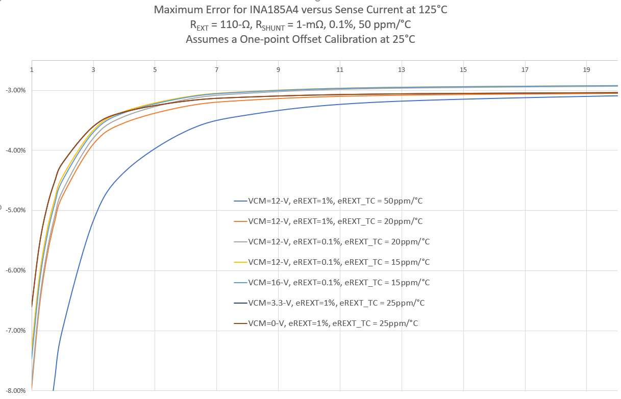
 Figure 6-3 Total Error Comparisons with
One-Point Offset Calibration at 25°C