SLYA062 June 2022 TMAG5110 , TMAG5110-Q1 , TMAG5111 , TMAG5111-Q1
2 Hall Element Orientation
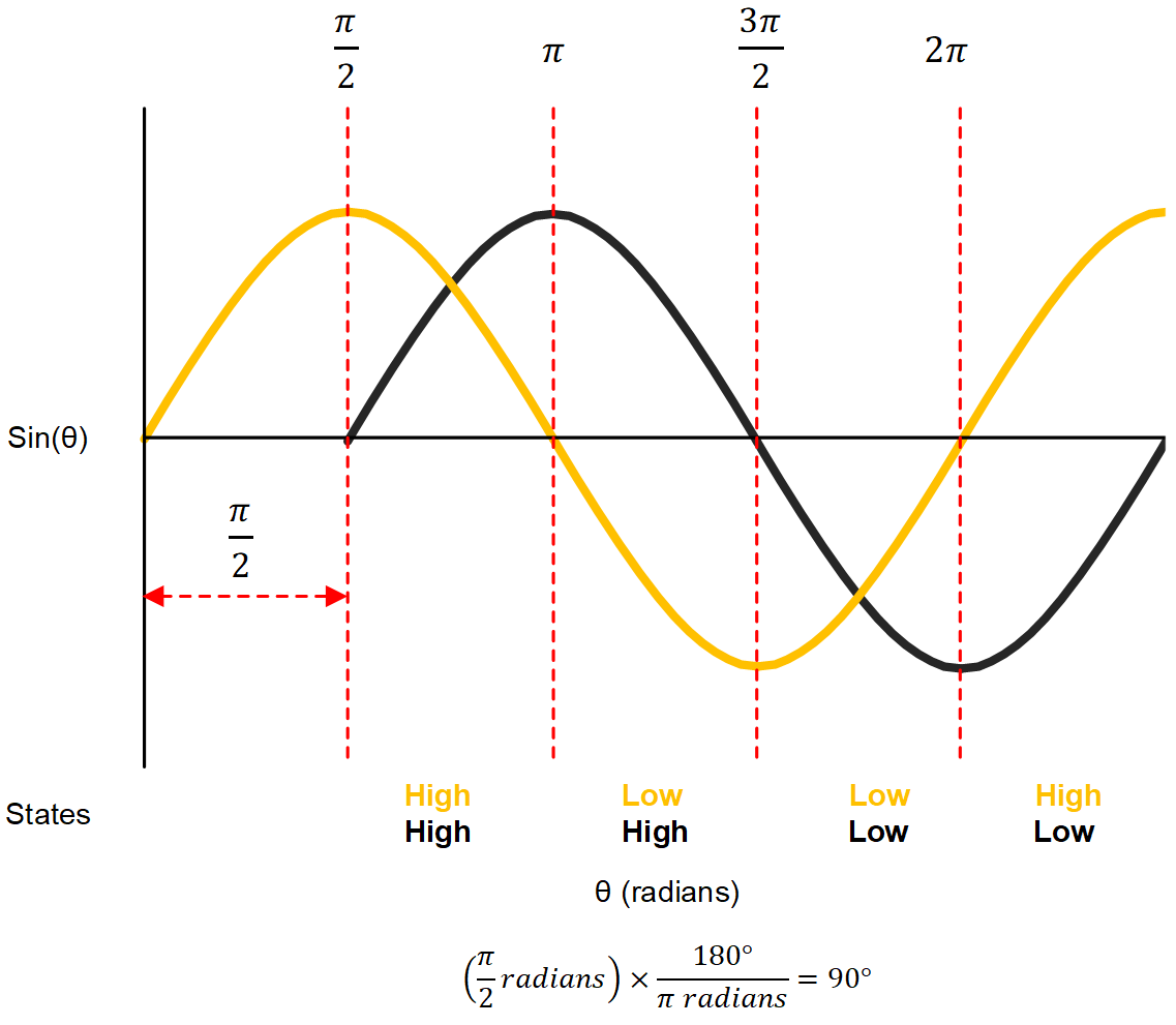
Position resolution is dictated by the orientation of the Hall element blocks within the device. To understand why, you must first recall the concept of phase. Figure 2-1 shows two sine waves which are similar in shape to the magnetic field measured by a Hall element in an encoding application. In Figure 2-1, the black curve lags behind the yellow curve. As the period is equivalent for both periodic signals, the lag is equivalent to the phase offset. Therefore, the black curve has a π/2=90° phase offset. Maintaining 90° offset is imperative for equal separation between latch states as indicated at the bottom of Figure 2-1.
 Figure 2-1 Phase Lag and Offset Example
Figure 2-2 shows what kind of output you might observe with a dual planar latch, assuming both Hall element blocks operate like a typical discrete latch.
The Hall elements are confined to a subregion of a small device package, therefore their physical separation will be miniscule. In most cases, this leads to signals with very small phase offsets and unequal state intervals as shown in the bottom of Figure 2-2.
Consequently, Figure 2-3 shows that dual planar devices typically monitor one Hall element block for speed and position, while another pin is used for direction. The speed element will generate a state change on one device output every time the detected polarity and magnitude crosses the opposing BOP or BRP threshold. The direction element also is similarly monitored; however, the BOP or BRP comparator output is kept internal to the device and fed to some other circuitry that compares both speed and direction signals. This setup can determine if the order of the rising and falling edges have reversed. This circuitry will then provide a device output that is high when the magnet is moving in one direction, or low when the magnet is moving in the opposite direction. Therefore, dual planar devices exhibit only two resolution steps from the speed hall element per pole pair traversed, which is half of what is possible for two Hall element block devices.
Despite the resolution limitation with a dual planar device, maximal resolution is still possible from a single 2D latch device. For a 2D device like the TMAG5110 or the TMAG5111 that has orthogonal planes, it is possible to get an unconditional 90° phase shift. Figure 2-4 illustrates why this is the case. Hall element 1 that is parallel to the magnet array measures a local maximum at a pole center, while the Hall element that is perpendicular to the magnet array measures a local minimum at a pole center.
Aside from resolution, device orientation relative to the encoding magnet can impact device functionality. To illustrate this point, Figure 2-5 shows a configuration in which a 2D latch will typically work while a dual planar will typically not. The dual planar fails to work in this configuration because the device can only sense along the axis orthogonal to the top of the package surface. In this instance, the magnetic field is mostly parallel to the Hall element plane and any vertical component that is normal to Hall elements and detectable is in phase. The 2D latch has 3 orthogonal sensing axes, therefore it is possible to detect the field components that are out of phase (see Figure 2-5).
To summarize the orientation limitations of the dual planar, Table 2-1 lists the configurations in which it may be difficult or impossible to successfully use dual planar. Figure 2-6, Figure 2-7, Figure 2-8, Figure 2-9, Figure 2-10, and Figure 2-11 show these various configurations listed in Table 2-1.
| Magnet Sensor Orientation | 2D | Dual Planar |
|---|---|---|
| Radial XY outer edge 1 | Possible | Not Recommended |
| Axial XY outer edge 1 | Possible | Not Recommended |
| Radial XY outer edge 2 | Possible | Not Recommended |
| Axial XY outer edge 2 | Possible | Possible |
| Radial ZX outer edge 1 | Possible | Possible |
| Axial ZX outer edge 1 | Possible | Possible |
| Radial ZX outer edge 2 | Possible | Not Recommended |
| Axial ZX outer edge 2 | Possible | Not Recommended |
| Radial ZY outer edge 1 | Possible | Not Recommended |
| Axial ZY outer edge 1 | Possible | Possible |
| Radial ZY outer edge 2 | Possible | Not Recommended |
| Axial ZY outer edge 2 | Possible | Possible |
| Radial XY side edge 1 | Possible | Not Recommended |
| Axial XY side edge 1 | Possible | Not Recommended |
| Radial XY side edge 2 | Possible | Not Recommended |
| Axial XY side edge 2 | Possible | Not Recommended |
| Radial ZX side edge 1 | Possible | Not Recommended |
| Axial ZX side edge 1 | Possible | Not Recommended |
| Radial ZX side edge 2 | Possible | Possible |
| Axial ZX side edge 2 | Possible | Possible |
| Radial ZY side edge 1 | Possible | Possible |
| Axial ZY side edge 1 | Possible | Not Recommended |
| Radial ZY side edge 2 | Possible | Possible |
| Axial ZY side edge 2 | Possible | Not Recommended |