SNAK009A April 2022 – February 2024 ADC128S102-SEP
2 SEE Mechanisms
The primary single-event effect (SEE) event of interest in the ADC128S102-SEP is the destructive single-event latch-up (SEL). From a risk and impact point-of-view, the occurrence of an SEL is potentially the most destructive SEE event and the biggest concern for space applications. The CMOS7 process node was used for the ADC128S102-SEP. CMOS circuitry introduces a potential for SEL susceptibility. SEL can occur if excess current injection caused by the passage of an energetic ion is high enough to trigger the formation of a parasitic cross-coupled PNP and NPN bipolar structure (formed between the p-sub and n-well and n+ and p+ contacts). The parasitic bipolar structure initiated by a single-event creates a high-conductance path (inducing a steady-state current that is typically orders-of-magnitude higher than the normal operating current) between power and ground that persists (is latched) until power is removed or until the device is destroyed by the high-current state. The process modifications applied for SEL-mitigation were sufficient as the ADC128S102-SEP exhibited no SEL with heavy-ions up to a of LETEFF = 43MeV-cm2 / mg at a fluence of 107 ions / cm2 and a chip temperature of 125°C.
This study was performed to evaluate the SEL effects with a bias voltage of 5.25V on VA and VD supply voltage. Heavy ions with LETEFF = 43MeV-cm2 / mg were used to irradiate the devices. Flux of 105 ions / s-cm2 and fluence of 107 ions / cm2 were used during the exposure at 125°C temperature.
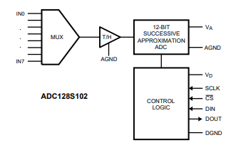
Figure 2-1 shows a functional block diagram for this device.
 Figure 2-1 Functional Block Diagram of the ADC128S102-SEP