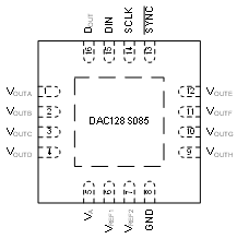
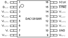
| DIN |
1 |
15 |
Digital Input |
Serial Data Input. Data is clocked into the 16-bit shift register on the falling edges of SCLK after the fall of SYNC. |
| DOUT |
2 |
16 |
Digital Output |
Serial Data Output. DOUT is utilized in daisy chain operation and is connected directly to a DIN pin on another DAC128S085. Data is not available at DOUT unless SYNC remains low for more than 16 SCLK cycles. |
| GND |
10 |
8 |
Ground |
Ground reference for all on-chip circuitry. |
| SCLK |
16 |
14 |
Digital Input |
Serial Clock Input. Data is clocked into the input shift register on the falling edges of this pin. |
| SYNC |
15 |
13 |
Digital Input |
Frame Synchronization Input. When this pin goes low, data is written into the DAC's input shift register on the falling edges of SCLK. After the 16th falling edge of SCLK, a rising edge of SYNC causes the DAC to be updated. If SYNC is brought high before the 15th falling edge of SCLK, the rising edge of SYNC acts as an interrupt and the write sequence is ignored by the DAC. |
| VA |
7 |
5 |
Supply |
Power supply input. Must be decoupled to GND. |
| VOUTA |
3 |
1 |
Analog Output |
Channel A Analog Output Voltage. |
| VOUTB |
4 |
2 |
Analog Output |
Channel B Analog Output Voltage. |
| VOUTC |
5 |
3 |
Analog Output |
Channel C Analog Output Voltage. |
| VOUTD |
6 |
4 |
Analog Output |
Channel D Analog Output Voltage. |
| VOUTE |
14 |
12 |
Analog Output |
Channel E Analog Output Voltage. |
| VOUTF |
13 |
11 |
Analog Output |
Channel F Analog Output Voltage. |
| VOUTG |
12 |
10 |
Analog Output |
Channel G Analog Output Voltage. |
| VOUTH |
11 |
9 |
Analog Output |
Channel H Analog Output Voltage. |
| VREF1 |
8 |
6 |
Analog Input |
Unbuffered reference voltage shared by Channels A, B, C, and D. Must be decoupled to GND. |
| VREF2 |
9 |
7 |
Analog Input |
Unbuffered reference voltage shared by Channels E, F, G, and H. Must be decoupled to GND. |
PAD
(WQFN only) |
— |
17 |
Ground |
Exposed die attach pad can be connected to ground or left floating. Soldering the pad to the PCB offers optimal thermal performance and enhances package self-alignment during reflow. |

