SNAS410F May 2008 – July 2016 DAC121S101QML-SP
PRODUCTION DATA.
- 1 Features
- 2 Applications
- 3 Description
- 4 Revision History
- 5 Pin Configuration and Functions
-
6 Specifications
- 6.1 Absolute Maximum Ratings
- 6.2 ESD Ratings
- 6.3 Recommended Operating Conditions
- 6.4 Thermal Information
- 6.5 DAC121S101QML-SP Electrical Characteristics DC Parameters
- 6.6 DAC121S101QML-SP Electrical Characteristics AC and Timing Characteristics
- 6.7 DAC121S101QML Electrical Characteristics Radiation Electrical Characteristics
- 6.8 DAC121S101QML-SP Electrical Characteristics Operating Life Test Delta Parameters TA at 25°C
- 6.9 Typical Characteristics
- 7 Detailed Description
- 8 Application and Implementation
- 9 Power Supply Recommendations
- 10Layout
- 11Device and Documentation Support
- 12Mechanical, Packaging, and Orderable Information
5 Pin Configuration and Functions
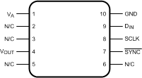
NAC Package
10-Pin CFP
Top View

Pin Functions
| PIN | I/O | DESCRIPTION | |
|---|---|---|---|
| NO. | NAME | ||
| 1 | VA | — | Power supply and reference input; must be decoupled to GND |
| 2 | N/C | — | No connect; pin not internally connected to die |
| 3 | N/C | — | No connect; pin not internally connected to die |
| 4 | VOUT | Output | DAC analog output voltage |
| 5 | N/C | — | No connect; pin not internally connected to die |
| 6 | N/C | — | No connect; pin not internally connected to die |
| 7 | SYNC | Input | Frame synchronization input for the data input. When this pin goes low, it enables the input shift register and data is transferred on the falling edges of SCLK. The DAC is updated on the 16th clock cycle unless SYNC is brought high before the 16th clock, in which case the rising edge of SYNC acts as an interrupt and the write sequence is ignored by the DAC. |
| 8 | SCLK | Input | Serial clock input; data is clocked into the input shift register on the falling edges of this pin. |
| 9 | DIN | Input | Serial data input; data is clocked into the 16-bit shift register on the falling edges of SCLK after the fall of SYNC. |
| 10 | GND | — | Ground reference for all on-chip circuitry |