SNAU260A October 2020 – February 2021 LMK5C33216
ADVANCE INFORMATION
- Trademarks
- 1Introduction
- 2EVM Quick Start
- 3EVM Configuration
-
4EVM Schematics
- 4.1 Power Supply Schematic
- 4.2 Power Distribution Schematic
- 4.3 LMK5C33216 and Input Reference Inputs IN0 to IN1 Schematic
- 4.4 Clock Outputs OUT0 to OUT3 Schematic
- 4.5 Clock Outputs OUT4 to OUT9 Schematic
- 4.6 Clock Outputs OUT10 to OUT15 Schematic
- 4.7 XO Schematic
- 4.8 Logic I/O Interfaces Schematic
- 4.9 USB2ANY Schematic
- 5EVM Bill of Materials
- 6Appendix A - TICS Pro LMK5C33216 Software
- 7Revision History
3 EVM Configuration
The LMK5C33216 is a highly configurable clock chip with multiple power domains, PLL domains, and clock input and output domains. To support a wide range of LMK5C33216 use cases, the EVM was designed with more flexibility and functionality than needed to implement the chip in a customer system application.
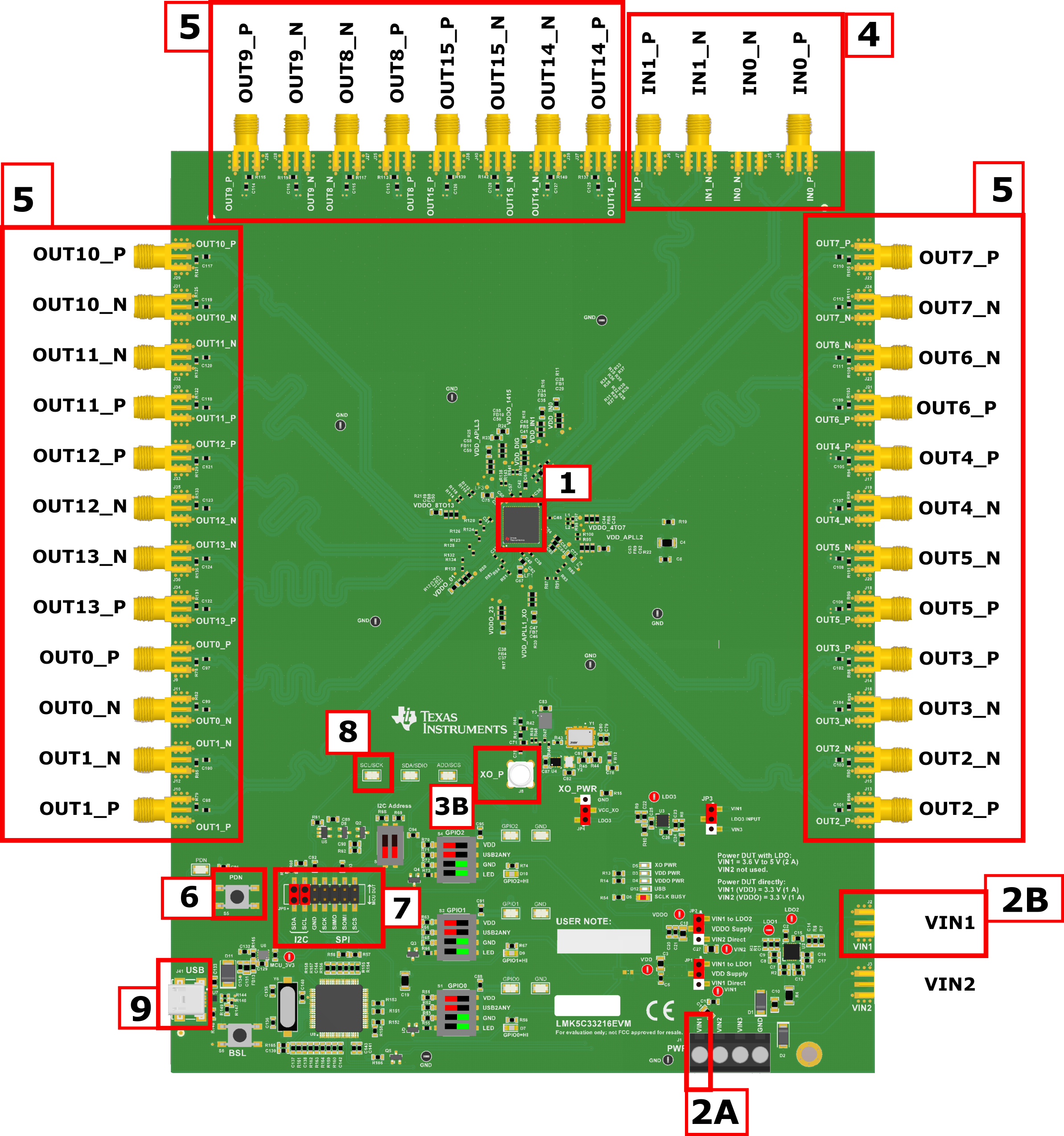
This section describes the power, logic, and clock input and output interfaces on the EVM, as well as how to connect, set up, and operate the EVM. Refer to Figure 4-1.
Table 3-1 Key Components REF DES and
Descriptions
| ITEM NO. | REF DES | DESCRIPTION | |
|---|---|---|---|
| 1 | U1 | LMK5C33216 DUT | |
| 2 | A | J1 (VIN1 terminal block header), or | External Supply, +5 V using default configuration. |
| B | J2 (VIN1 SMA) Not populated by default | ||
| 3 | A | Y1, or | |
| B | J8 | ||
| 4 | J4/5, J6/7 | SMA Ports for DUT Clock Inputs (IN0_P/N and IN1_P/N) | |
| 5 | J9/11, J10/12, J13/15, J14/16, J17/19, J18/20, J21/J23, J22/24, J25/27, J26/28, J29/31, J30/32, J33/35, J34/36, J37/39, J38/40 | SMA Ports for DUT Clock Outputs | |
| 6 | S5 | Normally open. Push button for DUT power down (PDN pin). Connect R76 to enable control of the PDN pin through the GUI | |
| 7 | JP5 | Jumper Header for I2C/SPI interface (MCU to DUT) | |
| 8 | D6 | SCL or SCK busy indication LED. | |
| 9 | J41 | USB Port for MCU | |
 Figure 3-1 Key Components - EVM Top
Side