SNAU274 December 2021
4 Board Layout
Figure 4-1 through Figure 4-3 illustrate the ADC128S102EVM board layout.
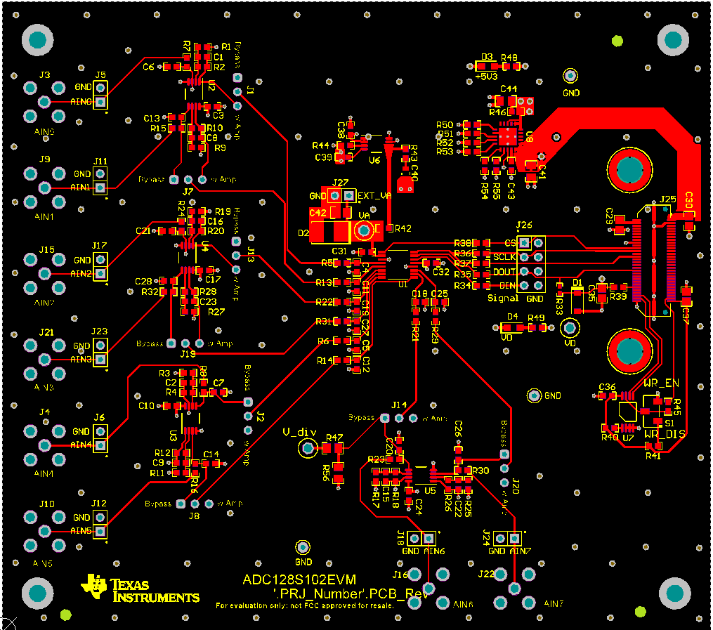 Figure 4-1 Top Layer and Assembly
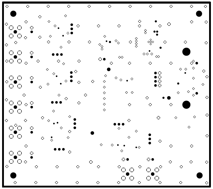 Figure 4-2 Inner Ground Layers 2 and
3
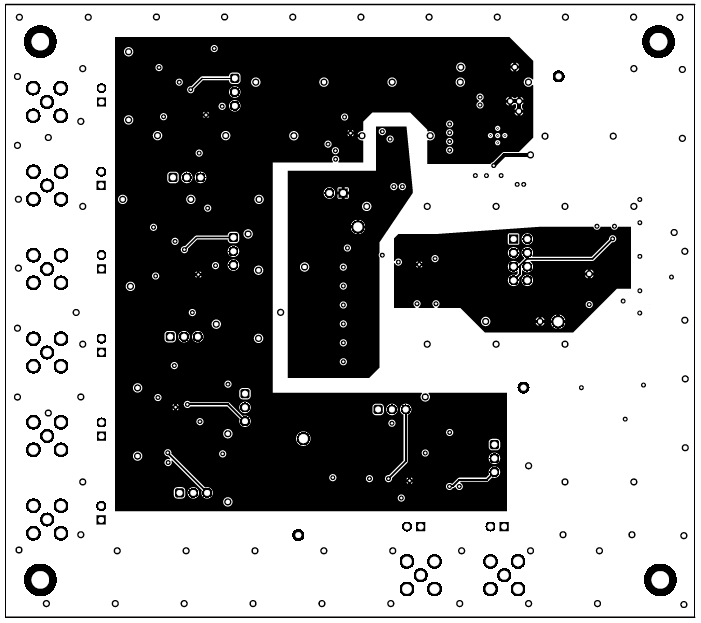 Figure 4-3 Bottom Layer
SNAU274 December 2021
Figure 4-1 through Figure 4-3 illustrate the ADC128S102EVM board layout.
 Figure 4-1 Top Layer and Assembly
 Figure 4-2 Inner Ground Layers 2 and
3
 Figure 4-3 Bottom Layer