SNAU274 December 2021
1.1 Analog Input Circuit
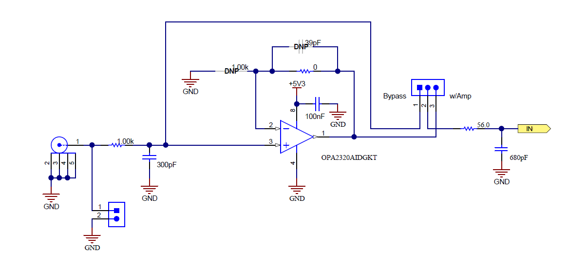
The EVM board has two subminiature version A (SMA) connectors, with six other footprints to populate the remaining SMA connectors (if required) to connect to the eight analog input channels. Shunt headers are also available in parallel with each respective SMA connector. As shown in Figure 1-2, each shunt header is connected to an analog input channel of the ADC128S102 through an operational amplifier (op amp) driver circuit. An input circuit is connected to each ADC analog input. The driver circuit consists of an initial RC circuit for noise filtering, followed by an OPA2320 (a dual-channel op amp configured, by default, as a buffer). The board has provisions to change the buffer circuit configuration, by removing the 0-Ω resistor and adding the desired RC combination. At the output of each op amp, is a 3-pin header that provides the option to bypass the buffer.
 Figure 1-2 Analog Input Circuit