SNAU278 July   2022


  1.   Abstract
  2.   Trademarks
  3. 1LMX2594PSEVM Evaluation Module
    1. 1.1 Evaluation Module Contents
    2. 1.2 Evaluation Setup Requirement
    3. 1.3 Resources
  4. 2Setup
    1. 2.1 Connection Diagram
    2. 2.2 Power Supply
    3. 2.3 Reference Clock
    4. 2.4 SYNC Input
    5. 2.5 RF Output
    6. 2.6 Programming
    7. 2.7 Evaluation Software
  5. 3Typical Measurement
    1. 3.1 Category 3 Synchronization
    2. 3.2 Phase Noise Improvement
  6. 4Schematic
  7. 5PCB Layout and Layer Stack-up
    1. 5.1 PCB Layer Stack-Up
    2. 5.2 PCB Layout
  8. 6Bill of Materials
  9. 7EVM Modification
  10. 8Troubleshooting Guide
  11. 9Reference PRO
    1. 9.1 Output Frequency Selection
    2. 9.2 Output Format Selection
    3. 9.3 Typical Output Characteristics
    4. 9.4 Firmware Update

Reference PRO

The Reference PRO board is used to program the LMX2594PSEVM and provide a clean reference clock to LMX2594PSEVM at the same time. The board has several control pins dedicated for control of output format, output frequency, and output enable control. These control pins are configurable through the jumpers by strapping the center pin to Vdd position or GND position. Connections from the Vdd position to the device supply or from the GND position to the ground plane are connected by 1.5-kΩ resistors. By default, the board is configured for 100-MHz LVPECL output. The power supply to Reference PRO is obtained from the PC through a USB connection.
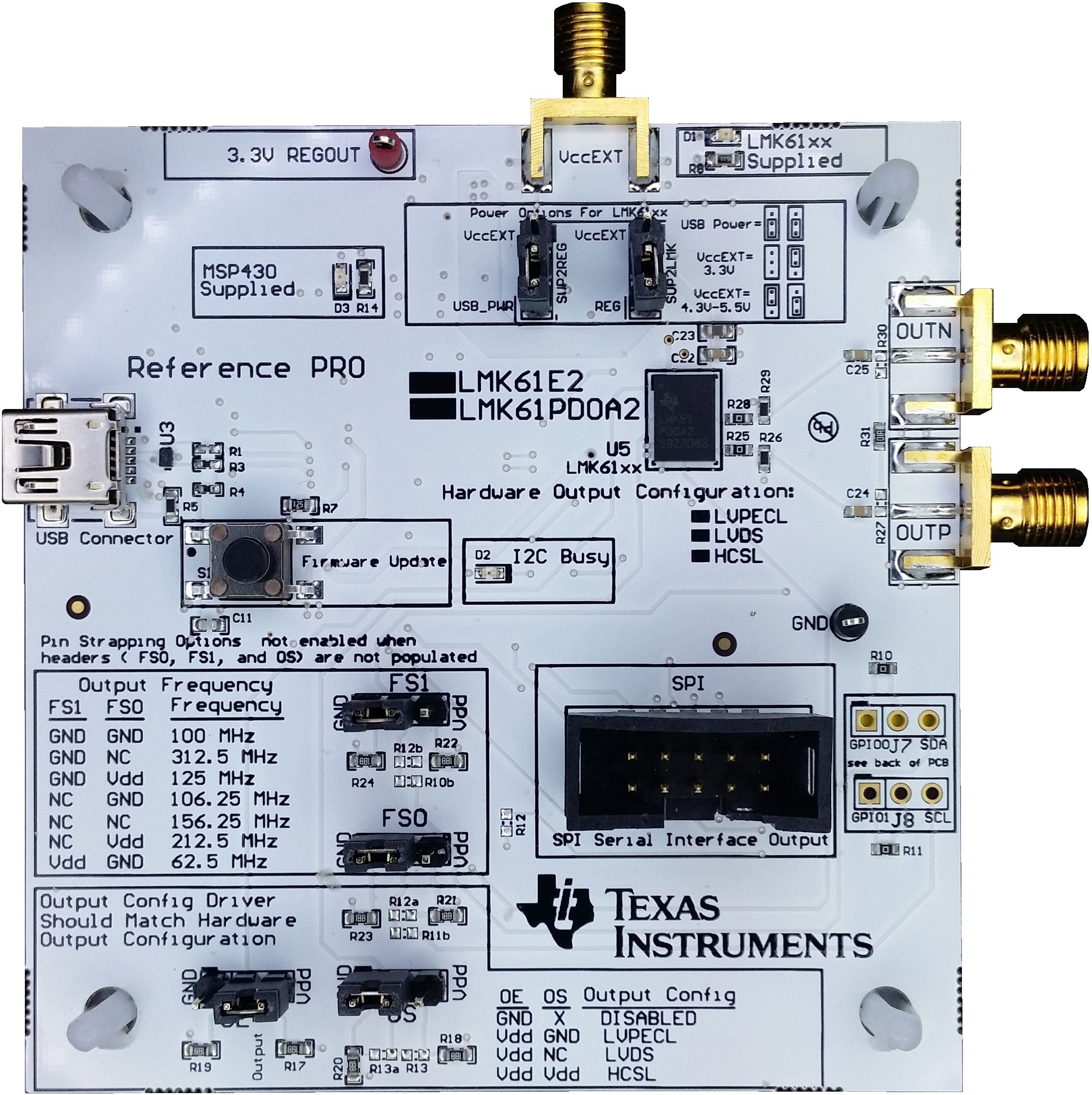
GUID-20220426-SS0I-VSGF-JTCJ-FZBXN7JVNNPH-low.jpgFigure 9-1 Reference PRO Board