SNAU279A July 2022 – September 2022
- Abstract
- Trademarks
- 1Introduction
- 2EVM Quick Start
- 3EVM Configuration
-
4EVM
Schematics
- 4.1 Power Supply Schematic
- 4.2 Alternative Power Supply Schematic
- 4.3 Power Distribution Schematic
- 4.4 LMK5B33414 and Input Reference Inputs IN0 to IN1 Schematic
- 4.5 Clock Outputs OUT0 to OUT3 Schematic
- 4.6 Clock Outputs OUT4 to OUT9 Schematic
- 4.7 Clock Outputs OUT10 to OUT13 and Clock Inputs IN2 and IN3 Schematic
- 4.8 XO Schematic
- 4.9 Logic I/O Interfaces Schematic
- 4.10 USB2ANY Schematic
- 5EVM Bill of Materials
-
6Appendix A - TICS Pro LMK5B33414 Software
- 6.1 Using the Start Page
- 6.2 Using the Status Page
- 6.3 Using the Input Page
- 6.4 Using APLL1, APLL2, and APLL3 Pages
- 6.5 Using the DPLL1, DPLL2, and DPLL3 Pages
- 6.6 Using the Validation Page
- 6.7 Using the GPIO Page
- 6.8 SYNC/SYSREF/1-PPS Page
- 6.9 Using the Outputs Page
- 6.10 EEPROM Page
- 6.11 Design Report Page
- 7Revision History
6.3 Using the Input Page
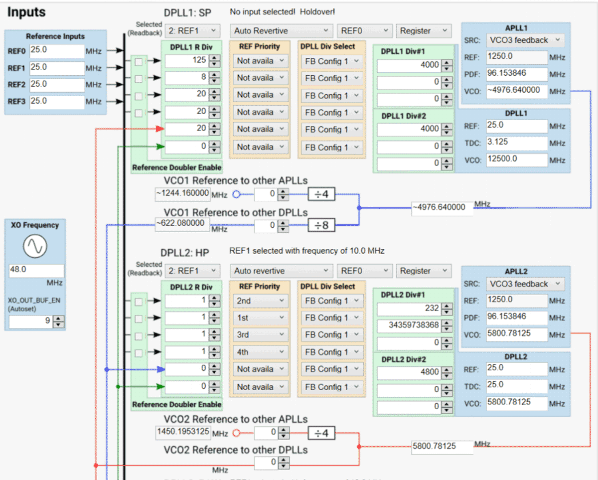
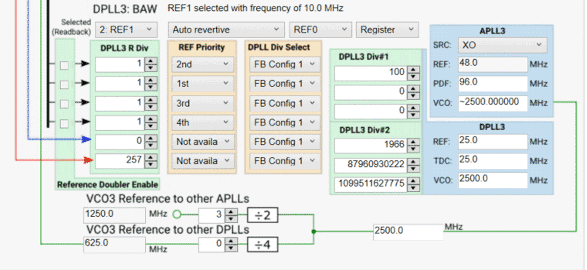
The Input page provides a high-level view of all the inputs for the device, the APLL frequencies, and DPLL frequencies of the device.
When the DPLL dividers and loop filter are calculated by running the script in step 7 on the Start page, this page displays the DPLL divider values which set the DPLL frequency. This example shows that the DPLL frequency is the exact desired frequency.
Each DPLL supports two sets of DPLL dividers which can be selected. At this time, the tool calculates the divider for FB Config 1 only. To use two different feedback dividers, the following procedure should be preformed.
- Div #1 settings may be copied into Div #2 settings and selected for use by the DPLL Div Select control.
- The references that require the Div #2 settings should be set to FB Config 2.
- You can run a second calculation (re-perform a run script, step 7 on Start page, of the DPLL), which will repopulate Div #1 settings with the new values for FB Config 1.
- Div #2 settings will remain the same as the ones initial copied over in step 1.
When using both feedback dividers, it is not required that the TDC rates are exactly the same, only that they are within ±5% for the two DPLL feedback configurations.
 Figure 6-9 APLL or DPLL Frequency Selection.
  Figure 6-10 PLL3 Input.