SNAU279A July 2022 – September 2022
- Abstract
- Trademarks
- 1Introduction
- 2EVM Quick Start
- 3EVM Configuration
-
4EVM
Schematics
- 4.1 Power Supply Schematic
- 4.2 Alternative Power Supply Schematic
- 4.3 Power Distribution Schematic
- 4.4 LMK5B33414 and Input Reference Inputs IN0 to IN1 Schematic
- 4.5 Clock Outputs OUT0 to OUT3 Schematic
- 4.6 Clock Outputs OUT4 to OUT9 Schematic
- 4.7 Clock Outputs OUT10 to OUT13 and Clock Inputs IN2 and IN3 Schematic
- 4.8 XO Schematic
- 4.9 Logic I/O Interfaces Schematic
- 4.10 USB2ANY Schematic
- 5EVM Bill of Materials
-
6Appendix A - TICS Pro LMK5B33414 Software
- 6.1 Using the Start Page
- 6.2 Using the Status Page
- 6.3 Using the Input Page
- 6.4 Using APLL1, APLL2, and APLL3 Pages
- 6.5 Using the DPLL1, DPLL2, and DPLL3 Pages
- 6.6 Using the Validation Page
- 6.7 Using the GPIO Page
- 6.8 SYNC/SYSREF/1-PPS Page
- 6.9 Using the Outputs Page
- 6.10 EEPROM Page
- 6.11 Design Report Page
- 7Revision History
6.2 Using the Status Page
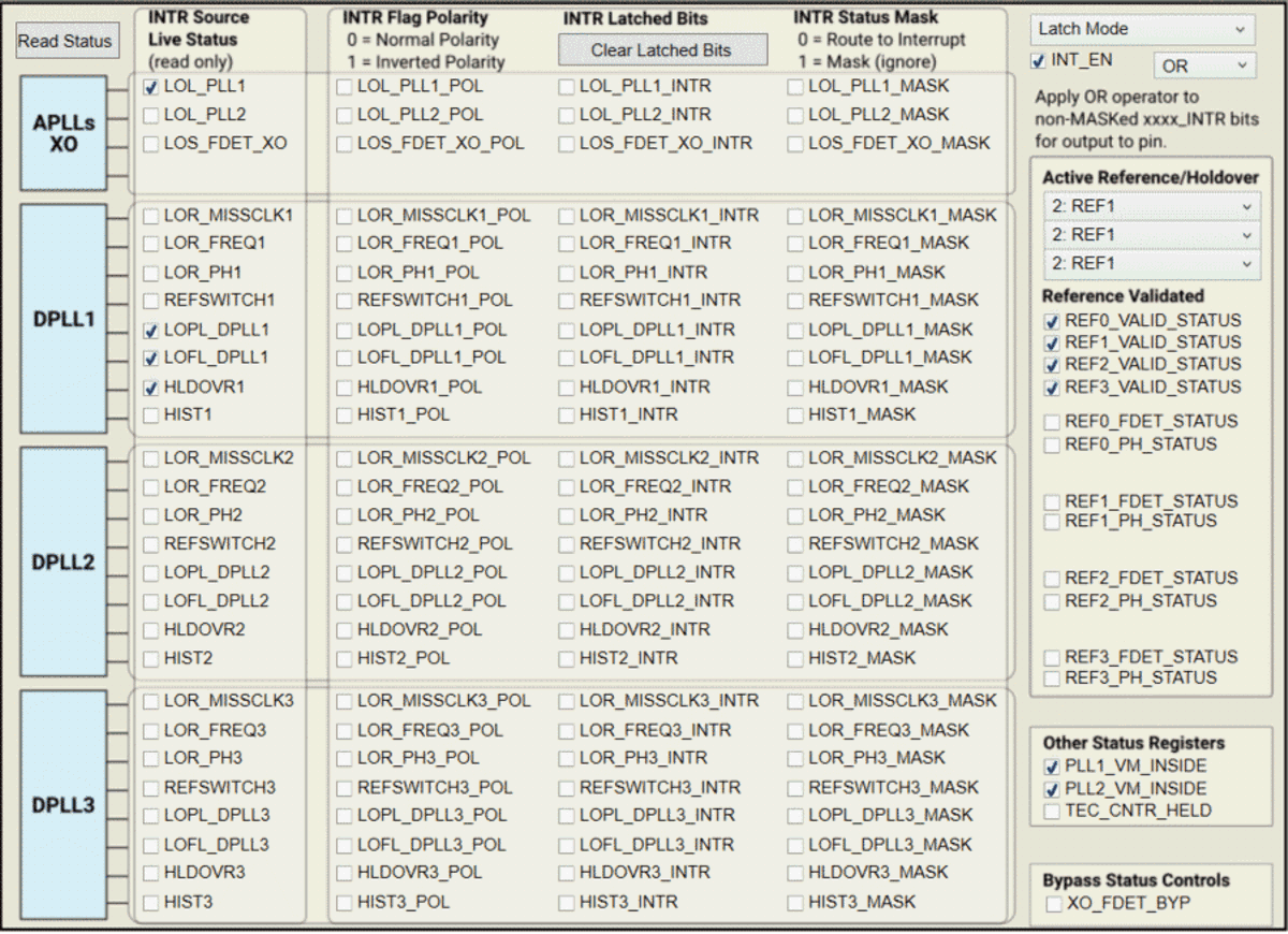
The Status page shows fields pertaining to the current status of the device. To update these fields, press the Read Status Bits button or the Read RO Regs button in the toolbar. The Read RO Regs button will read all read only registers which provides more information on other pages including the status fields but can take longer to read back. The read status bits just reads the status bits for this page.
For the DPLL to lock, a reference must be validated and selected in the Active Reference/Holdover and Reference Validated portions of the window shown in Figure 6-8.
As the DPLL locks, it is expected to see the LOPL_DPLLx as the last bit to become clear when the phase lock is acquired.
When INT_EN = 1, any live status flag which occurs will latch to the INTR Latched bit columns. These will remain asserted until the Clear Latched Bits button is pressed. This gives additional insight into the behavior of the device.
Press the Soft-chip reset button in the toolbar to reset the device and restart the lock.
 Figure 6-8 Status Page.