SNAU279A July 2022 – September 2022
- Abstract
- Trademarks
- 1Introduction
- 2EVM Quick Start
- 3EVM Configuration
-
4EVM
Schematics
- 4.1 Power Supply Schematic
- 4.2 Alternative Power Supply Schematic
- 4.3 Power Distribution Schematic
- 4.4 LMK5B33414 and Input Reference Inputs IN0 to IN1 Schematic
- 4.5 Clock Outputs OUT0 to OUT3 Schematic
- 4.6 Clock Outputs OUT4 to OUT9 Schematic
- 4.7 Clock Outputs OUT10 to OUT13 and Clock Inputs IN2 and IN3 Schematic
- 4.8 XO Schematic
- 4.9 Logic I/O Interfaces Schematic
- 4.10 USB2ANY Schematic
- 5EVM Bill of Materials
-
6Appendix A - TICS Pro LMK5B33414 Software
- 6.1 Using the Start Page
- 6.2 Using the Status Page
- 6.3 Using the Input Page
- 6.4 Using APLL1, APLL2, and APLL3 Pages
- 6.5 Using the DPLL1, DPLL2, and DPLL3 Pages
- 6.6 Using the Validation Page
- 6.7 Using the GPIO Page
- 6.8 SYNC/SYSREF/1-PPS Page
- 6.9 Using the Outputs Page
- 6.10 EEPROM Page
- 6.11 Design Report Page
- 7Revision History
6.5.1 DPLL DCO
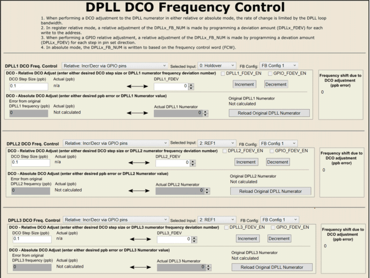
To use the DCO shift controls on a given DPLL, enter the DCO ppb step value into the DCO Step Size (ppb) box shown below. The entered step size will be used to calculate a frequency deviation that will be applied to the DPLL numerator. This frequency deviation is shown in the DPLLx_FDEV control. To perform the shift, you must press the increment or decrement button.
 Figure 6-18 DPLL DCO Controls.