SNAU296 December 2023 LMK5C33414A
- 1
- Abstract
- Trademarks
- 1Introduction
- 2EVM Quick Start
- 3EVM Configuration
-
4EVM
Schematics
- 4.1 Power Supply Schematic
- 4.2 Alternative Power Supply Schematic
- 4.3 Power Distribution Schematic
- 4.4 LMK5C33414A and Input References IN0 to IN3 Schematic
- 4.5 Clock Outputs OUT0 to OUT3 Schematic
- 4.6 Clock Outputs OUT4 to OUT9 Schematic
- 4.7 Clock Outputs OUT10 to OUT13 and Clock Inputs IN2 and IN3 Schematic
- 4.8 XO Schematic
- 4.9 Logic I/O Interfaces Schematic
- 4.10 USB2ANY Schematic
- 5EVM Bill of Materials
-
6Appendix A - TICS Pro LMK5C33414A Software
- 6.1 Using the Start Page
- 6.2 Using the Status Page
- 6.3 Using the Input Page
- 6.4 Using APLL1, APLL2, and APLL3 Pages
- 6.5 Using the DPLL1, DPLL2, and DPLL3 Pages
- 6.6 Using the Validation Page
- 6.7 Using the GPIO Page
- 6.8 SYNC/SYSREF/1-PPS Page
- 6.9 Using the Outputs Page
- 6.10 EEPROM Page
- 6.11 Design Report Page
6.8 SYNC/SYSREF/1-PPS Page
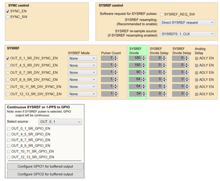
The SYNC/SYSREF/1-PPS page shows all the SYSREF block settings and allows the user to configure the GPIO1 or GPIO2 for continuous SYSREF or 1-PPS clock output.
The SYSREF divider output signals can be replicated on either GPIO1 and GPIO2 to provide additional single-ended, 3.3-V CMOS clocks after start-up if desired. To configure the SYSREF/1PPS output replication, the GPIO must be enabled as an output (GPIOx_OUTEN = 1) and one of the SYSREF output to GPIO replication sources must be active. The SYSREF replication source comes from any one of the SYSREF dividers in use from OUT0/1, OUT4/5, OUT6/7, OUT/9, OUT10/11 or OUT12/13 by register programming (OUT_x_y_SR_GPIO_EN = 1 and GPIO_SYSREF_SEL to the appropriate OUT_x_y). The GPIOx replicated SYSREF output is a continuous frequency. Pulsed SYSREF mode is not supported for the GPIOx replica outputs.
 Figure 6-21 SYNC/SYSREF/1-PPS Page