SNAU310 June   2024 LMKDB1102 , LMKDB1202


  1.   1
  2.   Description
  3.   Features
  4.   Applications
  5.   5
  6. 1Evaluation Module Overview
    1. 1.1 Introduction
    2. 1.2 Kit Contents
    3. 1.3 Specification
    4. 1.4 Device Information
  7. 2EVM Quick Start
    1. 2.1 Setup
    2. 2.2 EVM Measurements
  8. 3Hardware
    1. 3.1 EVM Configuration
      1. 3.1.1 Power Supply
      2. 3.1.2 Logic Input and Outputs
      3. 3.1.3 Clock Input
      4. 3.1.4 Clock Outputs
      5. 3.1.5 Status Outputs, LEDs, and Test Points
  9. 4Implementation Results
    1. 4.1 Typical Phase Noise Characteristic
  10. 5Hardware Design Files
    1. 5.1 Schematics
    2. 5.2 PCB Layouts
    3. 5.3 LMKDB1102EVM Bill of Materials (BOM)
    4. 5.4 LMKDB1202EVM Bill of Materials (BOM)
  11. 6Compliance Information
    1. 6.1 Compliance and Certifications
  12. 7Additional Information
    1. 7.1 Trademarks
  13. 8References

PCB Layouts


LMKDB1102EVM, LMKDB1202EVM Layer Stackup

Figure 5-8 Layer Stackup
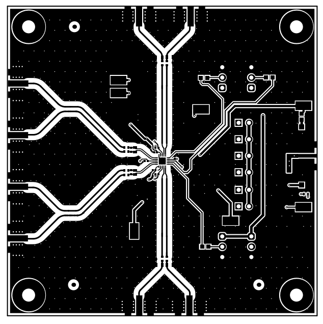
LMKDB1102EVM, LMKDB1202EVM Top Layer (CLKIN / CLKOUT
          Signals) Figure 5-9 Top Layer (CLKIN / CLKOUT Signals)
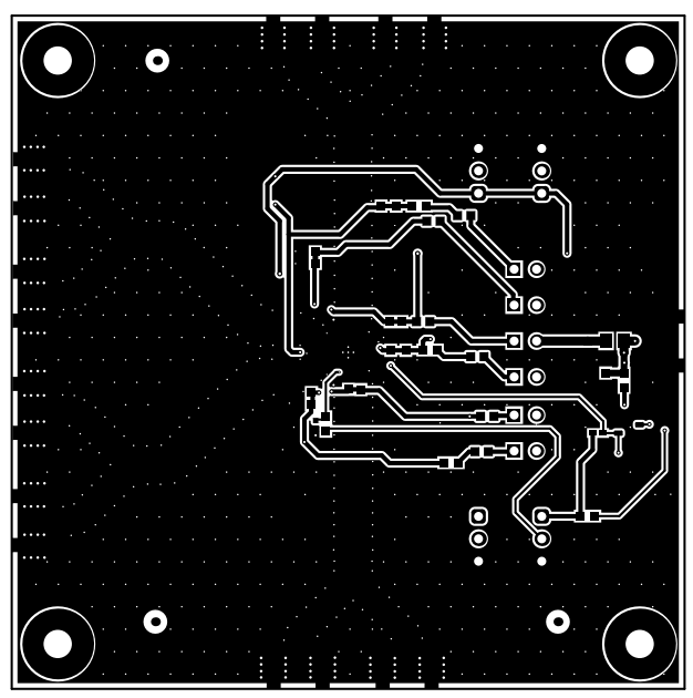
LMKDB1102EVM, LMKDB1202EVM Bottom Layer Figure 5-10 Bottom Layer
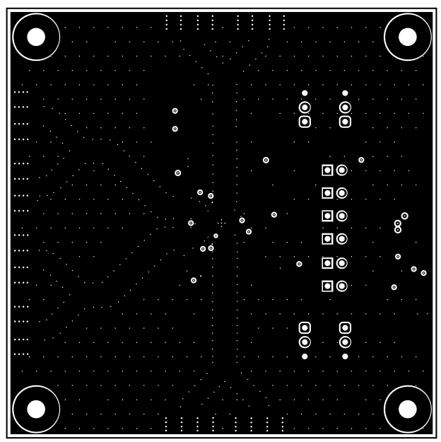
LMKDB1102EVM, LMKDB1202EVM GND Layer 1 Figure 5-11 GND Layer 1
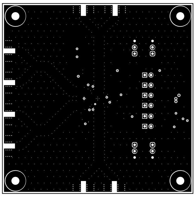
LMKDB1102EVM, LMKDB1202EVM GND 2 Layer Figure 5-12 GND 2 Layer