SNIA035A May 2020 – September 2024 TMP390-Q1
4 Pin Failure Mode Analysis (Pin FMA)
This section provides a failure mode analysis (FMA) for the pins of the TMP390-Q1 (SOT-563 package). The failure modes covered in this document include the typical pin-by-pin failure scenarios:
- Pin short-circuited to ground (see Table 4-2)
- Pin open-circuited (see Table 4-3)
- Pin short-circuited to an adjacent pin (see Table 4-4)
- Pin short-circuited to supply (see Table 4-5)
Table 4-2 through Table 4-5 also indicate how these pin conditions can affect the device as per the failure effects classification in Table 4-1.
| Class | Failure Effects |
|---|---|
| A | Potential device damage that affects functionality. |
| B | No device damage, but loss of functionality. |
| C | No device damage, but performance degradation. |
| D | No device damage, no impact to functionality or performance. |
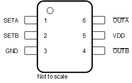
Figure 4-1 shows the TMP390-Q1 pin diagram. For a detailed description of the device pins, see the Pin Configuration and Functions section in the TMP390-Q1 data sheet.
 Figure 4-1 Pin Diagram
Following are the assumptions of use and the device configuration assumed for the pin FMA in this section:
- Device is the only target on the I2C bus
- External pull-up resistor on SCL and SDA pins
| Pin Name | Pin No. | Description of Potential Failure Effects | Failure Effect Class |
|---|---|---|---|
| SETA | 1 | SETA stuck low. Non-functional. False thermal limit triggers. | B |
| SETB | 2 | SETB stuck low. Non-functional. False thermal limit triggers. | B |
| GND | 3 | No effect. Normal operation. | D |
| OUTB | 4 | OUTB stuck low. Non-functional. False thermal limit triggers. | B |
| VDD | 5 | Device not powered. Device not functional. Observe that the absolute maximum ratings for all pins of the device are met, otherwise device damage is plausible. | A |
| OUTA | 6 | OUTA stuck low. Non-functional. False thermal limit triggers. | B |
| Pin Name | Pin No. | Description of Potential Failure Effect | Failure Effect Class |
|---|---|---|---|
| SETA | 1 | SETA stuck open. OUTA trip point is undetermined. False thermal limit can trigger. | B |
| SETB | 2 | SETB stuck open. OUTB trip point is undetermined. False thermal limit can trigger. | B |
| GND | 3 | Device functionality undetermined. Device not powered or connect to ground internally through alternate pin ESD diode and power up. | B |
| OUTB | 4 | OUTB stuck open. Non-functional. No thermal limit triggers. | B |
| VDD | 5 | Device functionality is undetermined. Device is not powered if all external analog and digital pins are held low. Device can power up through internal ESD diodes to V+ if voltages above the power-on reset threshold of the device are present on any of the analog or digital pins. |
B |
| OUTA | 6 | OUTA stuck open. Non-functional. No thermal limit triggers. | B |
| Pin Name | Pin No. | Shorted to | Description of Potential Failure Effect | Failure Effect Class |
|---|---|---|---|---|
| SETA | 1 | SETB | OUTA and OUTB trip point is undetermined. False thermal limit can trigger. | B |
| SETB | 2 | GND | SETB stuck low. Non-functional. False thermal limit triggers. | B |
| OUTB | 3 | VDD | OUTB stuck high. Non-functional. No thermal limit triggers. | B |
| VDD | 4 | OUTA | OUTA stuck high. Non-functional. No thermal limit triggers. | B |
| Pin Name | Pin No. | Description of Potential Failure Effect | Failure Effect Class |
|---|---|---|---|
| SETA | 1 | SETA stuck high. OUTA trip point is undetermined. False thermal limit can trigger. | B |
| SETB | 2 | SETB stuck high. OUTB trip point is undetermined. False thermal limit can trigger. | B |
| GND | 3 | Device functionality undetermined. Observe that the absolute maximum ratings for all pins of the device are met, otherwise device damage is plausible. | A |
| OUTB | 4 | OUTB stuck high. Non-functional. No thermal limit triggers. | B |
| VDD | 5 | No effect. Normal operation. | D |
| OUTA | 6 | OUTA stuck high. Non-functional. No thermal limit triggers. | B |