SNLA267A March 2019 – June 2019 DS90UB953-Q1 , DS90UB954-Q1 , DS90UB960-Q1
-
How to Design a FPD-Link III System Using DS90UB953-Q1 and DS90UB954-Q1
- Trademarks
- 1 Overview
- 2 Basic Design Rules
- 3 Designing the Link Between SER and DES
- 4 Designing Link Between SER and Image Sensor
- 5 Designing Link Between DES and ISP
- 6 Hardware Design
- 7
Appendix
- 7.1
Scripts
- 7.1.1 BIST Script
- 7.1.2 Example Sensor Initialization Script
- 7.1.3 CSI Enable and Port Forwarding Script
- 7.1.4 Enabling CMLOUT FPD3 RX Port 0 on 954
- 7.1.5 Remote Enabled SER GPIO Toggle Script
- 7.1.6 Local SER GPIO Toggle Script
- 7.1.7 Internal FrameSync on 953 GPIO1
- 7.1.8 External FrameSync on 953 GPIO0
- 7.1.9 SER GPIOs as Inputs and Output to DES GPIO
- 7.1.10 Pattern Generation on the 953 Script
- 7.1.11 Pattern Generation on the 954 Script
- 7.1.12 Monitor Errors for Predetermined Time Script
- 7.1.13 954 and 953 CSI Register Check Script
- 7.1.14 Time Till Lock Script on 953
- 7.2 Acknowledgments
- 7.1
Scripts
- Revision History
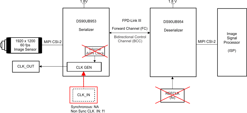
2.1.1.2 Non-Synchronous CLK_IN Mode
 Figure 5. Illustration of Non-Synchronous Mode With External Oscillator
 The second mode, non-synchronous CLK_IN, uses an external oscillator as a reference and generates the required clock for the FPD forward channel for that reference. Referring to Figure 5, the external clock must be fed into the CLK_IN pin (20) on the 953, running at a constant rate (f1) proportional to the REFCLK (f0), and a BC rate is then programmed to be less than or equal to 10 Mbps. Register 0x05, GENERAL_CFG, on the 953 holds parameters for the PLL clock control. Bits [6:4] of this register control the CLKIN divider. The CLKIN Divider can be divided by 1 or 2 by assigning these bits to 0b000 or 0b001, respectively. This division must be accounted for when calculating the FC rate which is shown in Table 5.