SNLA267A March 2019 – June 2019 DS90UB953-Q1 , DS90UB954-Q1 , DS90UB960-Q1
-
How to Design a FPD-Link III System Using DS90UB953-Q1 and DS90UB954-Q1
- Trademarks
- 1 Overview
- 2 Basic Design Rules
- 3 Designing the Link Between SER and DES
- 4 Designing Link Between SER and Image Sensor
- 5 Designing Link Between DES and ISP
- 6 Hardware Design
- 7
Appendix
- 7.1
Scripts
- 7.1.1 BIST Script
- 7.1.2 Example Sensor Initialization Script
- 7.1.3 CSI Enable and Port Forwarding Script
- 7.1.4 Enabling CMLOUT FPD3 RX Port 0 on 954
- 7.1.5 Remote Enabled SER GPIO Toggle Script
- 7.1.6 Local SER GPIO Toggle Script
- 7.1.7 Internal FrameSync on 953 GPIO1
- 7.1.8 External FrameSync on 953 GPIO0
- 7.1.9 SER GPIOs as Inputs and Output to DES GPIO
- 7.1.10 Pattern Generation on the 953 Script
- 7.1.11 Pattern Generation on the 954 Script
- 7.1.12 Monitor Errors for Predetermined Time Script
- 7.1.13 954 and 953 CSI Register Check Script
- 7.1.14 Time Till Lock Script on 953
- 7.2 Acknowledgments
- 7.1
Scripts
- Revision History
5.1.1 Using SER GPIOs From the DES
There are two ways to control the GPIOs of the SER using the deserializer: sending I2C commands across the back channel to the SER, or forwarding the SER GPIOs across the back channel using remote enable and controlling them from the DES. Because SER GPIOs are often connected to pins of the image sensor, it is important to understand how to control them.
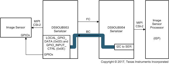
 Figure 15. Block Diagram of Controlling SER GPIOs Over BC
 As shown in Figure 15, the first method of controlling the serializer GPIOs is to send a write command over the back channel (BC) and control the appropriate registers on the 953. GPIO_INPUT_CTRL controls whether GPIO0-3 are configured as inputs or outputs. The first 4 bits [3:0] control whether they are used as inputs, and the last 4 bits [7:4] are used as outputs. This register has the address of 0x0E.
For example, the code below sends an I2C transaction over the BC using the 953 Alias ID, finds the GPIO_INPUT_CTRL register, and configures all four GPIOs on the 953 as outputs:
board.WriteI2C(953_Alias_ID,0x0E,0xF0)
Table 21. Example Using GPIO_INPUT_CTRL Register 0x0E for Local SER GPIO Control
| ADDR. | 0x0E[7:4] | 0x0E[3:0] |
|---|---|---|
| Bits | 1111 | 0000 |
| Desc. | Controls if GPIO3-0 are outputs | Controls if GPIO3-0 are inputs |
Furthermore, the LOCAL_GPIO_DATA (0x0D) register controls the SER GPIOs. The last 4 bits [7:4] of this register (GPIO_RMTEN) force the selected GPIO pins to be remotely controlled by the deserializer. These bits will not be used in this method. In addition, the first 4 bits [3:0] (GPIO_OUT_SRC) of the control the logical output of the GPIO registers. Note the corresponding GPIOs can only be changed when remote enable is disabled and the GPIOs are configured as outputs.
For example, the code below sends another I2C transaction over the BC using the 953 Alias ID, finds the LOCAL_GPIO_DATA register, and sets every SER GPIO to high. This is because the previous line of code set every GPIO to outputs—the last 4 bits for remote enable are 0, and the first 4 bits are set to logic 1:
board.WriteI2C(953_Alias_ID,0x0D,0x0F)
Table 22. Example Using LOCAL_GPIO_DATA Register 0x0D for Local SER GPIO Control
| ADDR. | 0x0D[7:4] | 0x0D[3:0] |
|---|---|---|
| Bits | 0000 | 1111 |
| Desc. | Enables remote control of SER GPIO3-0 | Controls logical outputs of GPIO3-0 |
An application of this process is described in Section 4.1.
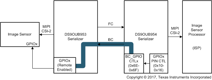
 Figure 16. Block Diagram of Controlling SER GPIOs Remotely
 As shown in Figure 16, the second method of controlling the serializer GPIOs is to remotely enable the SER GPIOs for access from the BC GPIO control of the DES. Then, the back channel GPIO control can be configured to mirror the DES GPIOs or different functions.
As mentioned before, the LOCAL_GPIO_DATA register controls the SER GPIOs. The last 4 bits [7:4] of this register (GPIO_RMTEN) force the selected GPIO pins to be remotely controlled by the deserializer. For example, the code below sends an I2C transaction over the BC using the 953 Alias ID, finds the GPIO_INPUT_CTRL register, and configures all four GPIOs on the 953 to be controlled by the DES:
board.WriteI2C(953_Alias_ID,0x0D,0xF0)
Table 23. Example Using LOCAL_GPIO_DATA Register 0x0D for Local SER GPIO Control
| ADDR. | 0x0D[7:4] | 0x0D[3:0] |
|---|---|---|
| Bits | 1111 | 0000 |
| Desc. | Enables remote control of SER GPIO3-0 | Controls logical outputs of GPIO3-0 |
Because the GPIOs are remote enabled, the GPIOs of the SER are forwarded to the DES, wait to be defined, and later send the data back to the SER. These forwarded GPIOs are stored on the DES in the form of BC GPIOs.
Table 24. BC_GPIO_CTL0 Registers From the 954 Data Sheet
| ADDR (HEX) | REGISTER NAME | BIT(S) | FIELD | TYPE | DEFAULT | DESCRIPTION |
|---|---|---|---|---|---|---|
| 0x6E | BC_GPIO_CTL0 | 7:4 | BC_GPIO1_SEL | RW | 0x8 | Back channel GPIO1 Select:
Determines the data sent on GPIO1 for the port back channel. 0xxx : Pin GPIOx where x is BC_GPIO1_SEL[2:0] 1000 : Constant value of 0 1001 : Constant value of 1 1010 : FrameSync signal 1011 - 1111 : Reserved |
| 3:0 | BC_GPIO0_SEL | RW | 0x8 | Back channel GPIO0 Select:
Determines the data sent on GPIO0 for the port back channel. 0xxx : Pin GPIOx where x is BC_GPIO0_SEL[2:0] 1000 : Constant value of 0 1001 : Constant value of 1 1010 : FrameSync signal 1011 - 1111 : Reserved |
Because the GPIOs are remote enabled, the GPIOs of the SER are now forwarded to the DES, wait to be defined, and later send the data to the SER. These forwarded GPIOs are stored on the DES in the form of BC GPIOs. The BC_GPIO_CTL register, with an address of 0x6E and 0x6F, controls the state of the forwarded GPIOs. For example, the first 4 bits [3:0] of 0x6E control the BC_GPIO0, while the last 4 bits [7:4] of 0x6E control the BC_GPIO1. Configuring these 4 bits will select one of many different functions, such as sending constant values of 0 or 1, internally generating Frame Sync signals, or following the values of a DES GPIO.
If the BC GPIOs are not defined by one of the internally generated functions, they must be linked to one of the seven different GPIOs on the 954. Because GPIOs can function as inputs or outputs, a signal defined by the GPIOs of the 954—and subsequently the BC GPIO of the DES—will be visible on GPIO pins of the 953.
For example, the below code will define GPIO1 of the SER as 1, and link the GPIO0 of the DES to the GPIO0 of the SER. To reiterate, probing the GPIO1 pin of the SER will show 1, while probing the GPIO0 pin of the SER will be the same as probing the GPIO0 pin of DES. Note that this will not require an I2C transaction across the BC:
board.WriteI2C(954_ID,0x6E,0x90)
Table 25. Example using BC_GPIO_CTL0 Register 0x6E for Remote SER GPIO Control
| ADDR. | 0x6E[7:4] | 0x6E[3:0] |
|---|---|---|
| Bits | 1001 | 0000 |
| Desc. | Determines data sent to SER GPIO1 (selected for constant value of 1) | Determines data sent to SER GPIO0 (selected to link to DES GPIO0) |
After forwarding the BC GPIOs to one of the DES GPIOs, the DES GPIOs can be configured as an output using the GPIOx_PIN_CTL with addresses of 0x10-0x16. In addition, the GPIOx_PIN_CTL has controls to select the source of the output generated to the GPIO. Bits [4:2] select the output source, such as RX Port 0, Device Status, and so forth. Bits [7:5] select the output based on what source was selected, such as the RX Port Lock indicator. Bits [1] and [0] control the logical output and output enable bits, respectively.
For example, the below code will make the DES GPIO0 an output for an internally generated FrameSync signal that is forwarded to SER GPIO0:
board.WriteI2C(954_ID,0x0F,0x00)
board.WriteI2C(954_ID,0x10,0x91)
An application of this process is explained in Section 5.1.2.