SNLA382 March 2021 DS250DF230
3.2 RTV (QFN) Layout Example
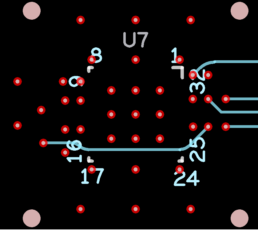
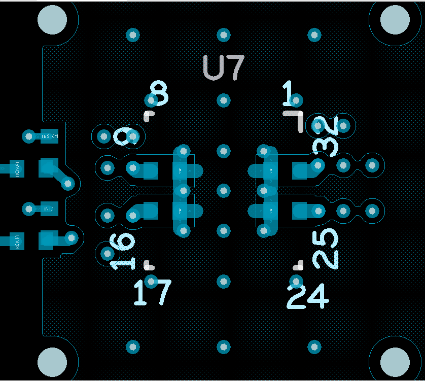
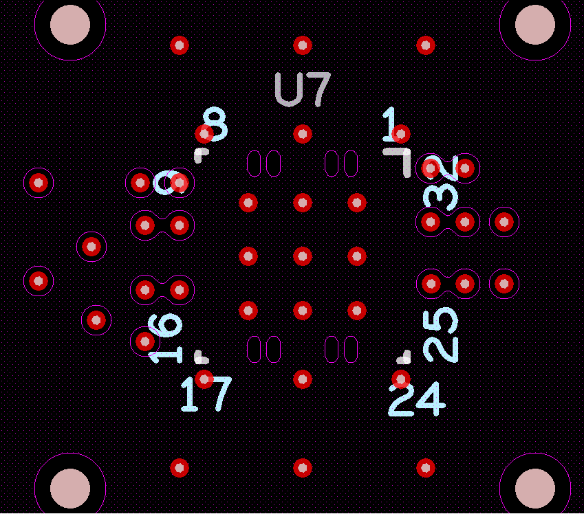
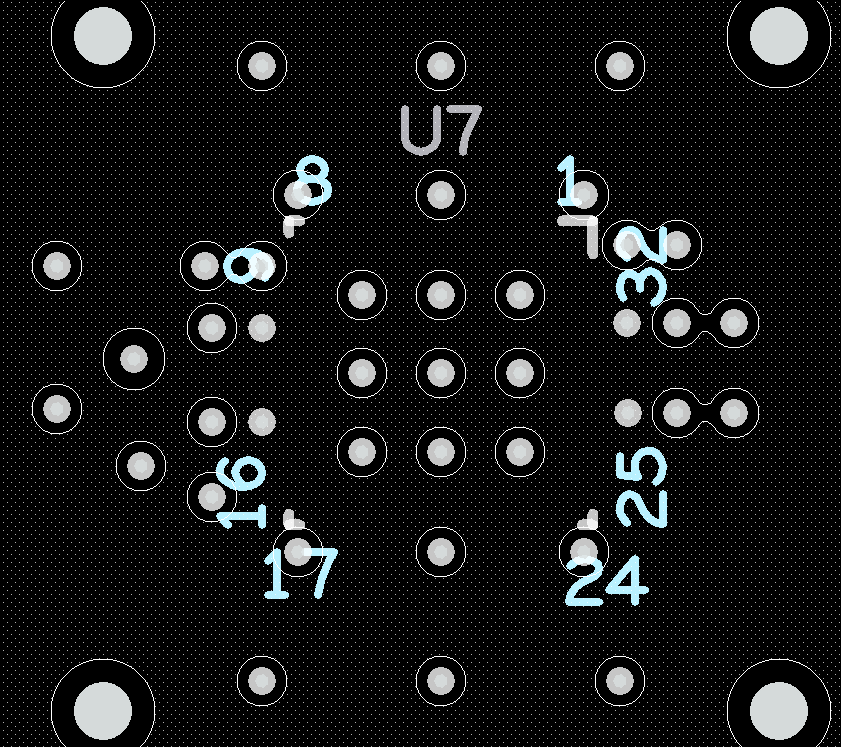
The example layout in this subsection demonstrates how all signals can be routed from the QFN using microstrip routing on a generic multi-layer stackup.
 Figure 3-1 Top Layer
 Figure 3-3 Internal Low-Speed
Signals
 Figure 3-5 Bottom Layer
 Figure 3-2 Layer 1 GND
 Figure 3-4 VDD Layer