SNOA951 June 2016 LDC1312 , LDC1312-Q1 , LDC1314 , LDC1314-Q1 , LDC1612 , LDC1612-Q1 , LDC1614 , LDC1614-Q1
- Inductive Sensing Touch-On-Metal Buttons Design Guide
3.1.4 Mounting Techniques
For effective operation of ToM button, the sensor PCB should be fixed at a constant offset from the metal surface. If the sensor PCB is not held firmly, then it could move or vibrate away from the metal surface, which could be misinterpreted as a button press or change the desired button sensitivity.
In many applications the sensor coil can be part of the main PCB and mounting holes can be used to align the sensor to the outline of the metal button. The height at which the metal button sits above the PCB will have the largest impact on the operating point of the LDC. In other applications where there is not much space for a monolithic PCB, the sensor may be put onto a flex PCB board and attached to the main PCB with a connector. The same mechanical design considerations must be taken into account as well as adding stiffeners to the sensor to prevent false detection. Some applications may also be restricted in mechanical arrangement, so that the distance between the sensor PCB and button panel cannot be reduced sufficiently. In such cases, a wire-wound surface-mount inductor may be used instead of a PCB coil.
For a standard FR4 PCB implementation, either of the two following assembly stack-ups are recommended:
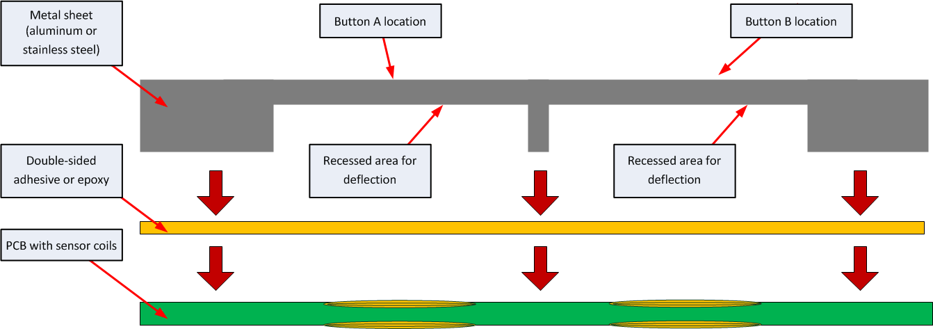
- A metal panel with a recessed area directly beneath the button on the bottom of the panel which can be created by either milling or etching a cavity into the metal, as shown in Figure 9. In this case, the left-over areas act as standoffs which support the PCB and ensure that there is room for metal deflection above the sensor coil. Double-sided adhesive (such as 3M 300LSE adhesive tape), or epoxy can be used to attach the PCB to the metal panel. If using adhesive tape, bubbles in the adhesive can form causing a non-uniform button response and potentially cause false detections. These air bubbles can be eliminated by either using adhesive with micro-channels or by adding non-plated vias to the PCB and applying force during the assembly process to compress the structure and force the air out and create a secure bond between the metal and PCB.
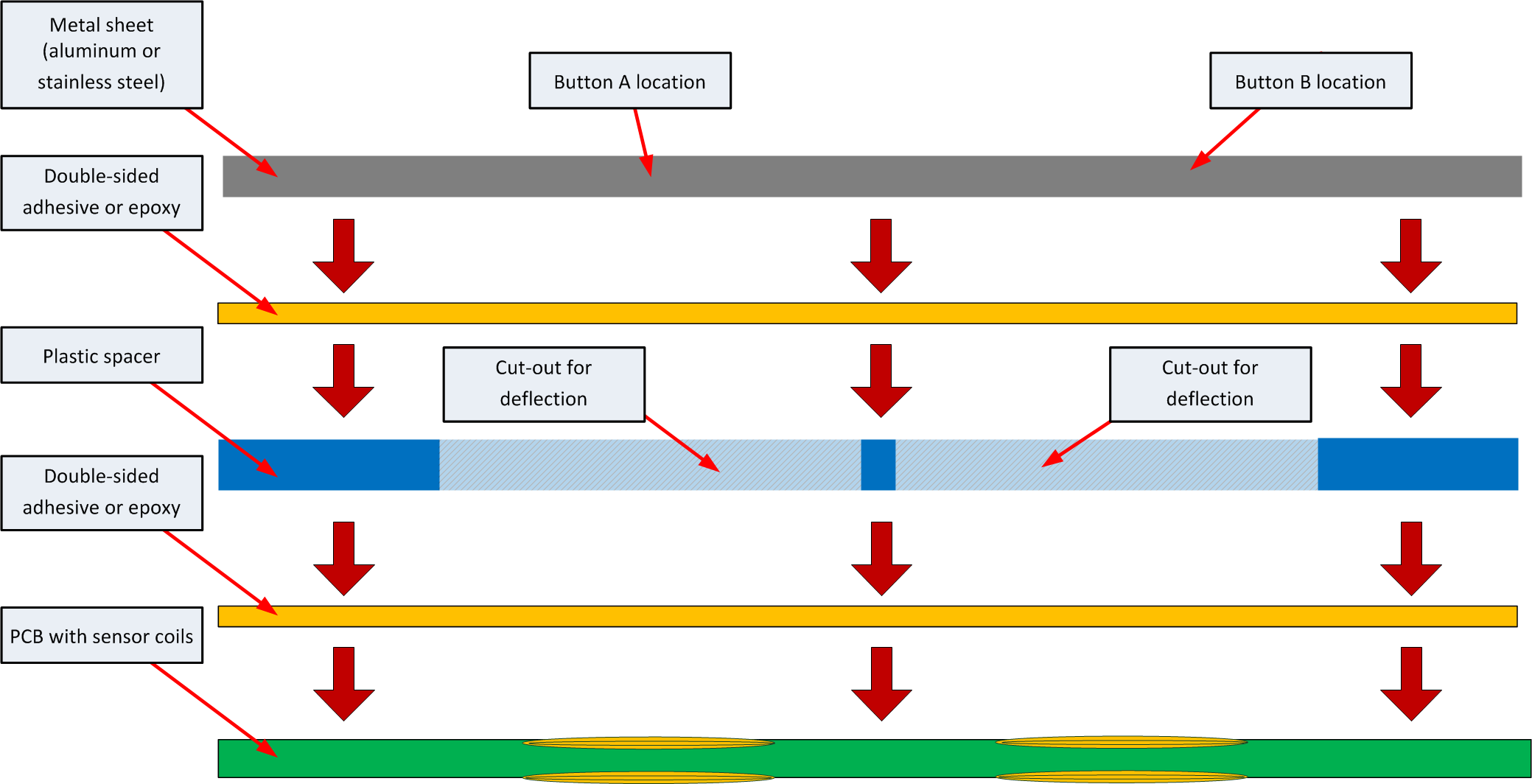
- A plastic spacer with cutouts can be placed between the metal panel and the PCB. This approach is useful in systems where a flat sheet of metal is used and it is not possible to do additional cutouts or milling to the metal. The spacer provides the necessary air gap between the metal sheet and the sensor to allow for deflection. Therefore, the cut-outs are of the same dimension and location as the button itself. Double-sided adhesive or epoxy can also be used to secure the assembly. Adding non-plated vias to both the PCB and the spacer that are aligned and adding sufficient pressure during the assembly process is important to remove the air bubbles that could accumulate and create undesired offsets or crosstalk between the channels.
 Figure 9. Assembly with Standoffs in the Metal Sheet
  Figure 10. Assembly with Plastic Spacer