SNOA951 June 2016 LDC1312 , LDC1312-Q1 , LDC1314 , LDC1314-Q1 , LDC1612 , LDC1612-Q1 , LDC1614 , LDC1614-Q1
- Inductive Sensing Touch-On-Metal Buttons Design Guide
3.1.2 Target Distance
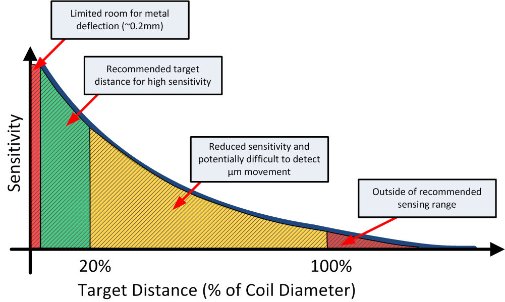
The nominal spacing between the inner metal surface and the PCB sensor is important to consider for both mechanical/assembly and electrical considerations. As the metal target approaches the sensor, the amount of inductance shift increases rapidly. The optimal target distance is where the sensor sensitivity is at its peak, but still has room for mechanical deflection. Metals that approach the sensor capture more of the electromagnetic field such that the highest sensitivity of the system occurs when the metal target is as close to the sensor as possible. However, to account for manufacturing tolerances and to ensure that there is still room for metal deflection, it is recommended for a nominal metal to sensor spacing be kept above 0.2mm. This spacing can be achieved by creating recessed area in the metal above the sensor for systems where the PCB is placed flush to the metal or by using a small spacer between the metal and the PCB sensor with a cutout to allow the metal to deflect, as shown in Figure 18. Additionally, the sensitivity rapidly decreases beyond 20% of the coil diameter, therefore it is recommended to place the sensor within this distance while leaving >0.2 mm of room for deflection, as shown in Figure 8.
 Figure 8. Optimal Target Distance