SNOAA62B February 2023 – October 2024 LMP7704-SP
7.1 Correlation Test Results
As part of an initial experiment to correlate the SET performance of the LMP7704-SP between test facilities, a new SEE characterization PCB was designed and populated with LMP7704-SP units. When a device was observed to fail under the beam, a detailed investigation commenced. Preliminary experimentation implied different PCB designs resulted in passing or failing behavior, but further investigation showed differences in decoupling capacitance to be the most significant underlying difference between the boards. When testing a coupon-style design with only 100nF decoupling capacitors localized, and the bulk capacitance isolated by several inches of trace length and several connectors worth of parasitic capacitance, the device was observed to pass repeatedly. Testing on a more conventional EVM-style of PCB, where multiple bulk capacitors were physically adjacent to the 100nF decoupling capacitors, led to device failure.
Oscilloscopes were used to monitor the voltage directly at the supply pins of the devices. These scope captures revealed the rapid initial supply voltage drop and slowly ramping recovery up associated with the ESD clamp activation, eventually leading to identification of the root cause. A sanity check performed on a covered unit (with the lid intact) showed the device packaging provided sufficient shielding to prevent the initial SET, and thus prevent an SEL. This implies the risk to most user applications is extremely low, though the vulnerability is still worth considering as part of standard failure mode and effects analysis. Testing was performed at both TAMU and MSU, and findings were shown to be replicable.
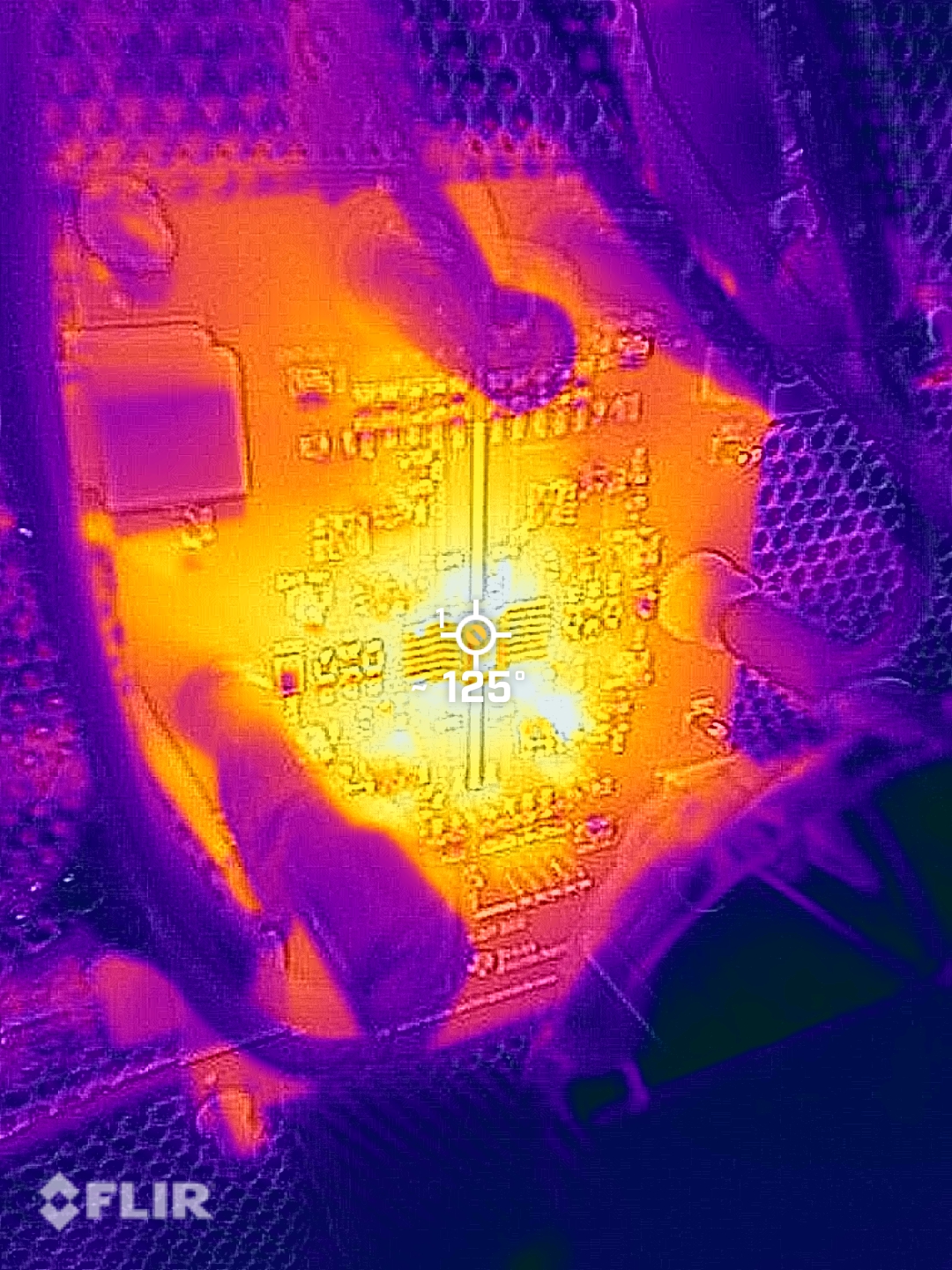
 Figure 7-1 Die Temperature
Verification with Thermal Camera, MSU
 Figure 7-2 Board Alignment for
Testing, TAMU
Figure 7-2 Board Alignment for
Testing, TAMUMultiple decoupling capacitor configurations were then explored, to identify a safe operating area for the device. When using only 100nF decoupling capacitors or less, no SEL was observed. Using a 100nF capacitor at the pin and 10μF bulk decoupling capacitor lead to failures in some cases, mostly correlating with higher power supply voltages and closer bulk capacitor placement. Using a 100nF capacitor at the pin and a 1μF bulk capacitor, or a 1μF and 10μF capacitor together, was more strongly correlated with SEL occurrence. The effect of capacitor composition or material was not experimentally studied due to limited component availability during the test sessions, but is expected to affect the response. Adding a sufficiently large series isolation resistance between the 100nF decoupling capacitor and any subsequent bulk capacitors was observed to prevent SEL.
As an experiment, one prototypical DUT was subjected to the ion stream repeatedly and under multiple test conditions. All decoupling capacitors were removed from the PCB. The supply voltage was slowly stepped from the minimum to the maximum value, both at room temp and at 125°C, to the point that a total exposure of approximately 340krad(Si) was accumulated. 100nF decoupling capacitors were reinstalled at the pins and testing was repeated, again passing to the maximum voltage and reaching an accumulated dose of 410krad(Si). 1μF parallel decoupling capacitors were added and the testing repeated, with a failure observed at 9V supply. By the time of the failure, the part had experienced nearly 500krad(Si) of total ionizing dose.