SNOK005 October 2024 LMP7704-SP
4.1 Input Offset Voltage Parametric Shift
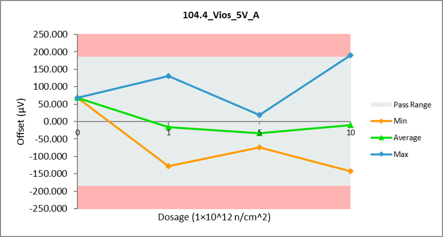
Input offset voltage (VOS) for the LMP7704-SP is specified as ±60μV typical and ±260μV maximum at TA = 25°C. The input offset voltage was measured at multiple supply voltages, with test limits of ±185μV for guardbanding purposes.
Three of the twelve devices exposed to neutron irradiation were found to have a measured input offset voltage outside of the guardbanded test limits, on one or more of the four device amplifier channels, for at least one of the VOS tests performed on the ATE. All measured values remained with the data sheet specified limits, for all devices. The values reported below represent the magnitude and directionality of the shift from the pre-exposure measurement, expressed in μV, for each device and condition. Full pre- and post-exposure data for all ATE tests performed are included in the report appendix. As a crude index, the data for each dose level are used to calculate the Bessel-corrected sample standard deviation (s) of the offset shift; s is found to increase as the cumulative dose increases.
| Unit | Supply | Channel A | Channel B | Channel C | Channel D | s |
|---|---|---|---|---|---|---|
| 1 | VS = 5V | +88.432 | +24.036 | +50.195 | -4.177 | 35.044 |
| VS = 10V | +79.624 | +18.513 | +38.832 | -5.127 | ||
| 2 | VS = 5V | +27.634 | +39.601 | -41.485 | +60.676 | |
| VS = 10V | +22.145 | +34.311 | -35.087 | +57.200 | ||
| 3 | VS = 5V | -61.277 | -14.743 | +16.797 | +3.580 | |
| VS = 10V | -52.567 | -14.465 | +11.481 | +2.171 | ||
| 4 | VS = 5V | -7.876 | -12.891 | +8.308 | -8.516 | |
| VS = 10V | -6.592 | -9.093 | +6.550 | -8.083 |
| Unit | Supply | Channel A | Channel B | Channel C | Channel D | s |
|---|---|---|---|---|---|---|
| 5 | VS = 5V | -25.547 | -118.428 | -38.656 | +3.755 | 66.673 |
| VS = 10V | -26.434 | -105.461 | -36.588 | +4.632 | ||
| 6 | VS = 5V | -19.562 | -4.832 | +13.177 | -7.609 | |
| VS = 10V | -18.817 | -0.652 | +13.181 | -4.783 | ||
| 7 | VS = 5V | -36.408 | +38.063 | -32.699 | +113.456 | |
| VS = 10V | -29.418 | +25.783 | -26.348 | +107.052 | ||
| 8 | VS = 5V | -26.330 | -72.764 | -8.161 | +185.890 | |
| VS = 10V | -25.182 | -69.251 | -4.635 | +175.764 |
| Unit | Supply | Channel A | Channel B | Channel C | Channel D | s |
|---|---|---|---|---|---|---|
| 9 | VS = 5V | +172.272 | -124.878 | -94.899 | +40.835 | 84.223 |
| VS = 10V | +160.339 | -114.584 | -87.128 | +31.696 | ||
| 10 | VS = 5V | +64.434 | +102.370 | -31.398 | +53.751 | |
| VS = 10V | +70.216 | +94.933 | -30.141 | +63.028 | ||
| 11 | VS = 5V | -75.925 | -142.616 | -12.038 | -83.020 | |
| VS = 10V | -71.388 | -137.099 | -13.083 | -72.343 | ||
| 12 | VS = 5V | -64.779 | +29.720 | +70.216 | -7.914 | |
| VS = 10V | -57.925 | +22.536 | +61.959 | -13.460 |
 Figure 4-1 Sample Input Offset Voltage NDD
Graph