SNOSD01D May 2015 – October 2016
PRODUCTION DATA.
- 1 Features
- 2 Applications
- 3 Description
- 4 Simplified Schematic
- 5 Revision History
- 6 Pin Configuration and Functions
- 7 Specifications
-
8 Detailed Description
- 8.1 Overview
- 8.2 Functional Block Diagram
- 8.3 Feature Description
- 8.4
Device Functional Modes
- 8.4.1 Measurement Modes
- 8.4.2 RP+L Measurement Mode
- 8.4.3 High Resolution L (LHR) Measurement Mode
- 8.4.4 Reference Count Setting
- 8.4.5 L-Only Measurement Operation
- 8.4.6 Minimum Sensor Frequency and Watchdog Setting
- 8.4.7 Low Power Modes
- 8.4.8 Status Reporting
- 8.4.9 Switch Functionality and INTB Reporting
- 8.5 Programming
- 8.6
Register Maps
- 8.6.1 Individual Register Listings
- 8.6.2 Register RP_SET (address = 0x01) [reset = 0x07]
- 8.6.3 Register TC1 (address = 0x02) [reset = 0x90]
- 8.6.4 Register TC2 (address = 0x03) [reset = 0xA0]
- 8.6.5 Register DIG_CONF (address = 0x04) [reset = 0x03]
- 8.6.6 Register ALT_CONFIG (address = 0x05) [reset = 0x00]
- 8.6.7 Register RP_THRESH_HI_LSB (address = 0x06) [reset = 0x00]
- 8.6.8 Register RP_THRESH_HI_MSB (address = 0x07) [reset = 0x00]
- 8.6.9 Register RP_THRESH_LO_LSB (address = 0x08) [reset = 0x00]
- 8.6.10 Register RP_THRESH_LO_MSB (address = 0x09) [reset = 0x00]
- 8.6.11 Register INTB_MODE (address = 0x0A) [reset = 0x00]
- 8.6.12 9.Register START_CONFIG (address = 0x0B) [reset = 0x01]
- 8.6.13 Register D_CONFIG (address = 0x0C) [reset = 0x00]
- 8.6.14 Register L_THRESH_HI_LSB (address = 0x16) [reset = 0x00]
- 8.6.15 Register L_THRESH_HI_MSB (address = 0x17) [reset = 0x00]
- 8.6.16 Register L_THRESH_LO_LSB (address = 0x18) [reset = 0x00]
- 8.6.17 Register L_THRESH_LO_MSB (address = 0x19) [reset = 0x00]
- 8.6.18 Register STATUS (address = 0x020 [reset = 0x00]
- 8.6.19 Register RP_DATA_LSB (address = 0x21) [reset = 0x00]
- 8.6.20 Register RP_DATA_MSB (address = 0x22) [reset = 0x00]
- 8.6.21 Register L_DATA_LSB (address = 0x23) [reset = 0x00]
- 8.6.22 Register L_DATA_MSB (address = 0x24) [reset = 0x00]
- 8.6.23 Register LHR_RCOUNT_LSB (address = 0x30) [reset = 0x00]
- 8.6.24 Register LHR_RCOUNT_MSB (address = 0x31) [reset = 0x00]
- 8.6.25 Register LHR_OFFSET_LSB (address = 0x32) [reset = 0x00]
- 8.6.26 Register LHR_OFFSET_MSB (address = 0x33) [reset = 0x00]
- 8.6.27 Register LHR_CONFIG (address = 0x34) [reset = 0x00]
- 8.6.28 Register LHR_DATA_LSB (address = 0x38) [reset = 0x00]
- 8.6.29 Register LHR_DATA_MID (address = 0x39) [reset = 0x00]
- 8.6.30 Register LHR_DATA_MSB (address = 0x3A) [reset = 0x00]
- 8.6.31 Register LHR_STATUS (address = 0x3B) [reset = 0x00]
- 8.6.32 Register RID (address = 0x3E) [reset = 0x02]
- 8.6.33 Register DEVICE_ID (address = 0x3F) [reset = 0xD4]
-
9 Application and Implementation
- 9.1
Application Information
- 9.1.1 TI Designs and Application Notes
- 9.1.2 Theory of Operation
- 9.1.3 RP+L Mode Calculations
- 9.1.4 LDC1101 RP Configuration
- 9.1.5 Setting Internal Time Constant 1
- 9.1.6 Setting Internal Time Constant 2
- 9.1.7 MIN_FREQ and Watchdog Configuration
- 9.1.8 RP+L Sample Rate Configuration With RESP_TIME
- 9.1.9 High Resolution Inductance Calculation (LHR mode)
- 9.1.10 LHR Sample Rate Configuration With RCOUNT
- 9.1.11 Setting RPMIN for LHR Measurements
- 9.1.12 Sensor Input Divider
- 9.1.13 Reference Clock Input
- 9.1.14 INTB Reporting on SDO
- 9.1.15 DRDY (Data Ready) Reporting on SDO
- 9.1.16 Comparator Functionality
- 9.2 Typical Application
- 9.1
Application Information
- 10Power Supply Recommendations
- 11Layout
- 12Device and Documentation Support
- 13Mechanical, Packaging, and Orderable Information
9 Application and Implementation
NOTE
Information in the following applications sections is not part of the TI component specification, and TI does not warrant its accuracy or completeness. TI’s customers are responsible for determining suitability of components for their purposes. Customers should validate and test their design implementation to confirm system functionality.
9.1 Application Information
9.1.1 TI Designs and Application Notes
The following resources contain additional information on LDC1101 operation, configuration, and system design:
- Inductive Linear Position Sensing Using the LDC1101
- Inductive Proximity Switch Using the LDC1101
- LDC Selection Guide Application Report
- LDC Sensor Design Application Report
- LDC Target Design Application Report
- Performing L Measurements from LDC DRDY Timing Application Report
- Optimizing L Measurement Resolution for the LDC161x and LDC1101 Application Report
- Measuring RP of an L-C Sensor for Inductive Sensing Application Report
- Setting LDC1312/4, LDC1612/4, and LDC1101 Sensor Drive Configuration Application Report
9.1.2 Theory of Operation
An AC current flowing through an inductor generates an AC magnetic field. If a conductive material, such as a metal object, is brought into the vicinity of the inductor, the magnetic field induces a circulating current (eddy current) on the surface of the conductor. The eddy current is a function of the distance, size, and composition of the conductor.
 Figure 46. Conductor in an AC Magnetic Field
The eddy current generates its own magnetic field, which opposes the original field generated by the inductor. This effect can be considered as a set of coupled inductors, where the inductor is the primary winding and the eddy current in the conductor represents the secondary winding. The coupling between the windings is a function of the inductor, and the resistivity, distance, size, and shape of the conductor.
To minimize the current required to drive the inductor, a parallel capacitor is added to create a resonant circuit, which oscillates at a frequency given by Equation 1 when energy is injected into the circuit. In this way, the LDC1101 only needs to compensate for the parasitic losses in the sensor, represented by the series resistance RS of the LC tank. The oscillator is then restricted to operating at the resonant frequency of the LC circuit and injects sufficient energy to compensate for the loss from RS.
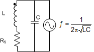 Figure 47. LC Tank
The resistance and inductance of the secondary winding caused by the eddy current can be modeled as a distant dependent resistive and inductive component on the primary side (coil). We can then represent the circuit as an equivalent parallel circuit, as shown in Figure 48.
 Figure 48. Equivalent Parallel Circuit
The value of RP can be calculated with:

where
- RS is the AC series resistance at the frequency of operation.
- C is the parallel capacitance
- L is the inductance
RP can be viewed as the load on the sensor driver; this load corresponds to the current drive needed to maintain the oscillation amplitude. The position of a target can change RP by a significant amount, as shown in Figure 49. The value of RP can then be used to determine the position of a conductive target. If the value of RP is too low, the sensor driver is not be able to maintain sufficient oscillation amplitude.
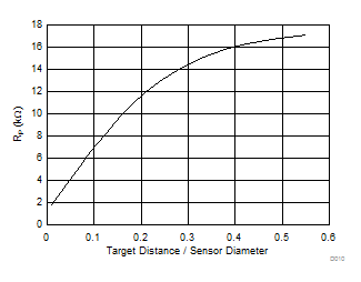 Figure 49. RP vs Target Distance for a 14-mm Diameter Sensor
9.1.3 RP+L Mode Calculations
For many systems which use the LDC1101, the actual sensor RP, sensor frequency, or sensor inductance is not necessary to determine the target position; typically the equation of interest is:
where
- RP_DATA is the contents of registers 0x21 and 0x22
- L_DATA is the contents of registers 0x23 and 0x24
These position equations are typically system dependent. For applications where the Sensor RP in Ωs needs to be calculated, use Equation 4:

where
- RPDATA is the contents of RP_DATA_MSB and RP_DATA_LSB (registers 0x21 and 0x22),
- RPMIN is the value set by RP_MIN in register RP_SET (register 0x01), and
- RPMAX is the value set by RP_MIN in register RP_SET (register 0x01).
For example, with device settings of:
- RPMIN set to 1.5 kΩ, and
- RPMAX set to 12 kΩ.
If RPDATA = 0x33F1 (register 0x21 = 0xF1 and register 0x22= 0x33), which is 13297 decimal, then the sensor RP = 1.824 kΩ.
If HIGH_Q_SENSOR (Register 0x01-b[7]) is set, then the equation is simply:

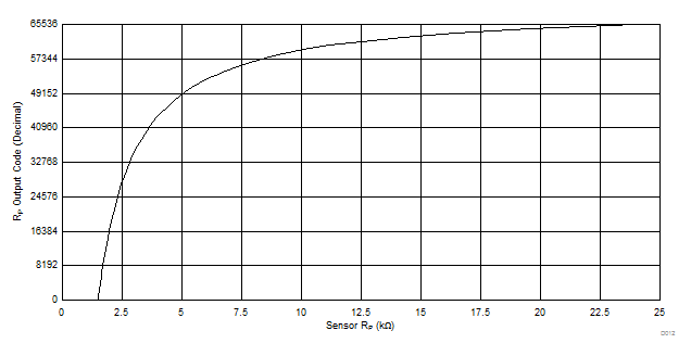 Figure 50. LDC1101 RP Transfer Curve with RPMIN = 1.5 kΩ and RPMAX = 24 kΩ
The sensor frequency in Hz can be calculated from Equation 6:

where
- ƒCLKIN is the frequency input to the CLKIN pin,
- L_DATA is the contents of registers 0x23 and 0x24, and
- RESP_TIME is the programmed response time in register 0x04.
The inductance in Henrys can then be determined from Equation 7:

where
- CSENSOR is the fixed sensor capacitance in Farads, and
- ƒSENSOR is the measured sensor frequency, as calculated in Equation 6 above.
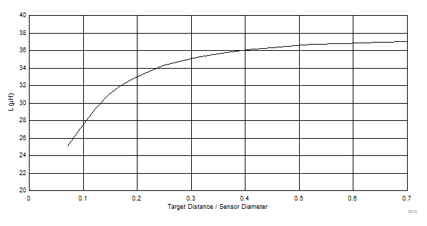 Figure 51. Inductance vs Normalized Target Distance for an Example Sensor
9.1.4 LDC1101 RP Configuration
Setting the RP_MIN and RP_MAX parameters is necessary for proper operation of the LDC1101; the LDC1101 may not be able to effectively drive the sensor with incorrect settings, as the sensor amplitude will be out of the valid operation region. The LDC1101EVM GUI and the LDC Excel® tools spreadsheet (http://www.ti.com/lit/zip/slyc137) can be used to calculate these parameters in an efficient manner.
For RP measurements, the following register settings must be set as follows:
- ALT_CONFIG.LOPTIMAL(register 0x05-bit0) = 0
- D_CONFIG.DOK_REPORT (register 0x0C-bit0) = 0
- Ensure that the sensor characteristics are within the Sensor boundary conditions:
- 500 kHz < ƒSENSOR < 10 MHz
- 100 pF < CSENSOR < 10 nF
- 1 µH < LSENSOR < 500 µH
- Measure the sensor’s resonance impedance with minimal target interaction (RPD∞). The minimal target interaction occurs when the target is farthest away from the sensor for axial sensing solutions or when the target coverage of the sensor is at a minimum for rotational or lateral sensing. Select the appropriate setting for RPMAX (register 0x01-bits [5:4]):
- Measure the sensor’s resonance impedance with the target closest to the sensor (RPD0) as required by the application. Select the largest RPMIN setting that satisfies:
- RPMIN < 0.8 × RPD0
- If the required RPMIN is smaller than 750 Ω, RPD0 must be increased to be compliant with this boundary condition. This can be done by one or more of the following:
- increasing ƒSENSOR
- increasing the minimum distance between the target and the sensor
- reducing the RS of the sensor by use of a thicker trace or wire
- Check if the worst-case Sensor quality factor QMIN = RpMIN × √(CSENSOR/LSENSOR) is within the device operating range:
- 10 ≤ QMIN ≤ 400
- If QMIN < 10, for a fixed ƒSENSOR, increase CSENSOR and decrease LSENSOR.
- If QMIN > 400, for a fixed ƒSENSOR, decrease CSENSOR and increase LSENSOR.
- Alternatively the user may choose to not change the current Sensor parameters, but to increase Rp_D0.
RPD∞ ≤ RPMAX ≤ 2RPD∞
If the RP of the sensor is greater than 75 kΩ, RP measurement accuracy may be improved by setting HIGH_Q_SENSOR to 1.
9.1.5 Setting Internal Time Constant 1
RP Measurements require configuration of the TC1 and TC2 registers. There are several programmable capacitance and resistance values. Set Time Constant 1 based on minimum sensor frequency:

where
- ƒSENSOR-MIN is the minimum sensor frequency encountered in the system; typically this occurs with no target present.
- VAMP is sensor amplitude of 0.6V,
- R1 is the programmed setting for TC1.R1 (register 0x03-bits[4:0]), and
- C1 is the programmed setting for TC1.C1 (register 0x03-bits[7:6])
The acceptable range of R1 is from 20.6 kΩ to 417.4 kΩ. If several combinations of R1 and C1 are possible, TI recommends using the largest capacitance setting for C1 that fits the constraints of Equation 8, as this will provide improved noise performance.
9.1.6 Setting Internal Time Constant 2
Set the Time Constant 2 (register 0x03) using Equation 9:
where
- CSENSOR is the parallel capacitance of the sensor.
- RP_MIN is the LDC1101 setting determined in LDC1101 RP Configuration (for example, use 1.5 kΩ when RP_SET.RP_MIN = b110),
- R2 is the programmed setting for TC2.R2 (register 0x03-bits[5:0]), and
- C2 is the programmed setting for TC2.C2 (register 0x03-bits[7:6]).
The acceptable range of R2 is from 24.60 kΩ to 834.8 kΩ. If several combinations of R2 and C2 are possible, TI recommends programming the larger capacitance setting for C2 that fits the constraints of Equation 9, as this will provide improved noise performance.
9.1.7 MIN_FREQ and Watchdog Configuration
The LDC1101 includes a watchdog timer which monitors the sensor oscillation. While in active mode, if no sensor oscillation is detected, the LDC1101 sets STATUS.NO_SENSOR_OSC (register 0x20:bit7), and attempt to restart the oscillator. This restart resets any active conversion.
The watchdog waits an interval of time based on the setting of DIG_CONF.MIN_FREQ (register 0x04:bits[7:4]). The MIN_FREQ setting is also used to configure the start-up of oscillation on the sensor. Select the DIG_CONF.MIN_FREQ (register 0x04-bits[7:4]) setting closest to the minimum sensor frequency; this setting is used for internal watchdog timing. If the watchdog determines the sensor has stopped oscillating, it reports the sensor has stopped oscillating in STATUS. NO_SENSOR_OSC (register 0x20-bit7). If the DIG_CONF.MIN_FREQ is set too low, then the LDC1101 takes a longer time interval to report that the sensor oscillation has stopped.
If the DIG_CONF.MIN_FREQ is set too high, then the watchdog may incorrectly report that the sensor has stopped oscillating and attempt to restart the sensor oscillation.
When the watchdog determines that the sensor has stopped oscillating, the LHR conversion results will contain 0xFFFFFF.
9.1.8 RP+L Sample Rate Configuration With RESP_TIME
The RP+L sample rate can be adjusted by setting by DIG_CONF.RESP_TIME (register 0x04:bits[2:0]). The Response time can be configured from 192 to 6144 cycles of the sensor frequency. Higher values of Response time have a slower sample rate, but produce a higher resolution conversion.

For applications which require only RP measurements, it is not necessary to apply a reference frequency on the CLKIN pin. If there is to be no signal input on CLKIN, is recommended to tie CLKIN to ground in this situation. The L and LHR measurements will return 0.
9.1.9 High Resolution Inductance Calculation (LHR mode)
For many systems which use the LDC1101, the actual sensor frequency or sensor inductance is not necessary to determine the target position. Should the sensor frequency in Hz need to be determined, use Equation 11:

where
- LHRDATA is the contents of registers 0x38, 0x39, and 0x3A,
- LHROFFSET is the programmed contents of registers 0x32 and 0x33,
- SENSOR_DIV is the contents of LHR_CONFIG.SENSOR_DIV (register 0x34-bit[1:0]), and
- ƒCLKIN is the frequency input to the CLKIN pin: ensure that it is within the specified limits of 1 MHz to 16 MHz.
Note that LHR_DATA=0x0000000 indicates a fault condition or that the LDC1101 has never completed an LHR conversion.
The inductance in Henrys can then be determined from the sensor frequency with Equation 12:

where
- CSENSOR is the fixed sensor capacitance, and
- ƒSENSOR is the measured sensor frequency, as calculated above.
Example with the device set to:
- LHR_OFFSET = 0x00FF (register 0x32 = 0xFF, and 0x33 = 0x00)
- ƒCLKIN = 16 MHz
- SENSOR_DIV = b’01 (divide by 2)
and the conversion result is:
LHR_DATA = 0x123456 (register 0x38 = 0x56, register 0x39 = 0x34,register 0x3A = 0x12)
Then entering LHR_DATA = 0x123456 = 1193046 (decimal) into Equation 11:

Results in ƒSENSOR = 2.400066 MHz.
9.1.10 LHR Sample Rate Configuration With RCOUNT
The conversion time represents the number of reference clock cycles used to measure the sensor frequency. The LHR mode conversion time is set by the Reference count in LHR_RCOUNT.RCOUNT (registers 0x30 and 0x31). The LHR conversion time is:

The 55 is due to post-conversion processing and is a fixed value. The reference count value must be chosen to support the required number of effective bits (ENOB). For example, if an ENOB of 13 bits is required, then a minimum conversion time of 213 = 8192 clock cycles is required. 8192 clock cycles correspond to a RCOUNT value of 0x0200.
Higher values for RCOUNT produce higher resolution conversions; the maximum setting, 0xFFFF, is required for full resolution.
9.1.11 Setting RPMIN for LHR Measurements
Configure the RP measurement as shown previously for L measurements. If only L measurements are necessary, then the RP measurement can be disabled by setting:
- ALT_CONFIG.LOPTIMAL(register 0x05-bit0) = 1
- D_CONFIG.DOK_REPORT (register 0x0C-bit0) = 1
Setting these bits disable the sensor modulation used by the LDC1101 to measure RP and can reduce L measurement noise. When the RP modulation is disabled, the LDC1101 drives a fixed current level into the sensor. The current drive is configured by RP_SET.RPMIN (address 0x01:bits[2:0]). The sensor amplitude must remain between 0.25 Vpk and 1.25 Vpk for accurate L measurements. Use Table 36 to determine the appropriate RPMIN setting, based on the variation in sensor RP. If multiple RPMIN values cover the Sensor RP, use the higher current drive setting. The equation to determine sensor amplitude is:

Table 36. LHR RPMIN Settings when Sensor RP Modulation is Disabled
| RPMIN SETTING | RPMIN FIELD VALUE | SENSOR DRIVE (μA) |
MINIMUM SENSOR RP (kΩ) |
MAXIMUM SENSOR RP (kΩ) |
|---|---|---|---|---|
| 0.75 kΩ | b111 | 600 | 0.53 | 1.65 |
| 1.5 kΩ | b110 | 300 | 1.1 | 3.3 |
| 3 kΩ | b101 | 150 | 2.1 | 6.5 |
| 6 kΩ | b100 | 75 | 4.2 | 13.1 |
| 12 kΩ | b011 | 37.5 | 8.4 | 26.2 |
| 24 kΩ | b010 | 18.7 | 16.9 | 52.4 |
| 48 kΩ | b001 | 9.4 | 33.9 | 105 |
| 96 kΩ | b000 | 4.7 | 67.9 | 209 |
For example, with a sensor that has an RP which can vary between 2.7 kΩ to 5 kΩ, the appropriate setting for RPMIN would be 3 kΩ (RP_SET.RPMIN = b101). For more information on sensor RP and sensor drive, refer to Configuring Inductive-to-Digital-Converters for Parallel Resistance (RP) Variation in L-C Tank Sensors(SNAA221).
9.1.12 Sensor Input Divider
The reference clock frequency should be greater than 4 times the sensor frequency for optimum measurement resolution:
For higher sensor frequencies, this relationship may not be realizable without the sensor divider. Set the sensor divider to an appropriate value to produce an effective reduction in the sensor frequency:
9.1.13 Reference Clock Input
Use a clean, low jitter, 40-60% duty cycle clock input with an amplitude swing within the range of VDD and GND; proper clock impedance control, and series or parallel termination is recommended. The rise and fall time should be less than 5 ns. Do not use a spread-spectrum or modulated clock.
For optimum L measurement performance, it is recommended to use the highest reference frequency (16 MHz). LHR conversions do not start until a clock is provided on CLKIN.
9.1.14 INTB Reporting on SDO
INTB is a signal generated by the LDC1101 that reports a change in device status. When INTB_MODE.INTB2SDO=1 (register 0x0A:bit7), INTB is multiplexed onto the SDO pin. Once the reporting is enabled, select the desired signal to report by setting INTB_MODE.INTB_FUNC (register 0x0A:bit[5:0]).
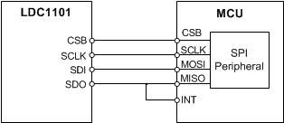 Figure 52. SDO/INTB Connection to MCU
For many microcontrollers, the MISO signal on the SPI peripheral cannot provide the desired interrupt functionality. One method to use the INTB functionality is to connect a second GPIO which triggers on a falling edge, as shown in Figure 51. Table 37 describes the signal functionality that can be programmed onto INTB.
Table 37. INTB Signal Options
| SIGNAL | INTB_FUNC (0x0A:bit[5:0]) |
FUNCTIONALITY | SWITCH OUTPUT TYPE |
|---|---|---|---|
| LHR Data Ready (LHR-DRDY) | b10’0000 | Indicates new High-Resolution Inductance (LHR) conversion data is available. | Latching |
| L_HI_LO | b01’0000 | L Comparator with hysteresis | Hysteresis |
| L_TH_HI | b00’1000 | Latching L High threshold compare | Latching |
| RP+L Data Ready (RPL-DRDY) | b00’0100 | Indicates new RP+L conversion data is available. | Pulse |
| RP_HI_LO | b00’0010 | RP Comparator with hysteresis | Hysteresis |
| RP_TH_HI | b00’0001 | Latching RP High threshold compare | Latching |
| None | b00’0000 | No INTB reporting – SDO pin only provides SDO functionality. | N/A |
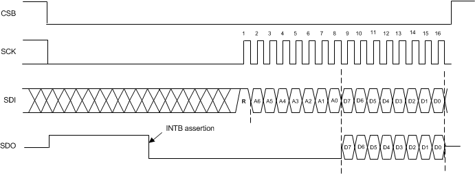 Figure 53. Example INTB Signal on SDO
When INTB_MODE.INTB2SDO (register 0x0A:bit7) = 0, the SDO pin is in a Hi-Z state until the 8th falling edge of SCLK after CSB goes low. When INTB reporting is enabled by setting INTB_MODE.INTB2SDO = 1, after CSB goes low, the SDO pin goes high and remains high until:
- the event configured by INTB_MODE.INTB_FUNC occurs,
- an SPI read transaction is initiated, or
- CSB is deasserted (pulled high)
9.1.15 DRDY (Data Ready) Reporting on SDO
Completion of a conversion can be indicated on the SDO pin by reporting the DRDY signal – there is a conversion complete indicator for the RP+L conversion (RPL-DRDY), and a corresponding conversion complete indicator for the LHR mode (LHR-DRDY).
When LHR-DRDY or RPL-DRDY is reported on SDO, the SDO pin is asserted on completion of a conversion. While in this mode, conversion data can be corrupted if a new conversion completes while reading the output data registers. To avoid data corruption, it is important to retrieve the conversion rates via SPI quicker than the shortest conversion interval, and to ensure that the data is retrieved before a new conversion could possibly complete.
When INTB is reporting RPL-DRDY, if CSB is held low for longer than one conversion cycle, INTB is deasserted approximately 100 ns to 2 µs prior to the completion of each conversion. The deassertion time is proportional to 1/ƒSENSOR.
When INTB is reporting LHR-DRDY, if CSB is held low for longer than one conversion cycle, INTB asserts on completion of the first conversion and remain low – and it remains asserted until cleared. To clear the LHR_DRDY signal, read the LHR_DATA registers.
 Figure 54. Reporting RPL-DRDY on INTB/SDO
 Figure 55. Reporting LHR-DRDY on INTB/SDO
Note that the conversion interval for an LHR measurement is asynchronous to the conversion interval for an RP+L measurement, therefore the LHR-DRDY signal cannot be used to determine when to read RP+L conversion results, and vice versa.
9.1.16 Comparator Functionality
The LDC1101 provides comparator functionality, in which the RP+L conversion results can be compared against two thresholds. The results of each RP and L conversion can be compared against programmable thresholds and reported in the STATUS register. Note that the LHR conversion results cannot be used for comparator functionality.
In addition, the INTB signal can be asserted or deasserted when the conversion results increase above a Threshold High or decreases below a Threshold Low registers. In this mode, the LDC1101 essentially behaves as a proximity switch with programmable hysteresis. The threshold HI settings must be programmed to a higher value than the threshold LO registers (for example, if RP_THRESH_LO is set to 0x2000, RP_THRESH_HI must programmed to 0x2001 or higher).
Either Latching and non-latching functions can be reported on INTB/SDO. The INTB signal can report a latching signal or a continuous comparison for each conversion result.
The Threshold setting registers (address 0x06:0x09 and 0x16:0x19) can be changed while the LDC1101 is in active conversion mode. It is recommended to change the register values using an extended SPI transaction as described in SPI Programming, so that the register updates can be completed in a shorter time interval. This functionality enables the LDC1101 to operate as a dynamic tracking switch. LDC1101 output codes can be readout in < 4 μs, and the set of active thresholds can be updated in <6 μs. It is not recommended to update the threshold registers more often than once per conversion interval of the LDC1101 (that is, do not change the threshold register values multiple times in a single conversion interval).
To clear a latched INTB signal, set INTB_MODE = 0x80; it is not necessary for the LDC1101 to be in Sleep mode to clear the latched output; the INTB_MODE can be changed while the LDC1101 is in active mode. After clearing the latched output, re-enabling the INTB_FUNC can be done while in active mode.
Table 38. Comparator Options
| FUNCTION | THRESHOLD HIGH | THRESHOLD LOW | STATUS REPORTING |
INTB/SDO REPORTING |
|---|---|---|---|---|
| RP Comparator with hysteresis | RP_THRESH_HI (registers 0x06 and 0x07) |
RP_THRESH_LO (registers 0x08 and 0x09) |
RP_HI_LON (bit 4) |
RP_HI_LO (INTB_MODE:INTB_FUNC=b00’0010) |
| RP High threshold only (Latching) | RP_THRESH_HI (registers 0x06 and 0x07) |
N/A | RP_HIN (bit 5) |
RP_TH_HI (INTB_MODE:INTB_FUNC=b00’0001) Note that INTB/SDO will latch. |
| L Comparator with hysteresis | L_THRESH_HI (registers 0x16 and 0x17) |
L_THRESH_LO (registers 0x18 and 0x19) |
L_HI_LON (bit 2) |
L_HI_LO (INTB_MODE:INTB_FUNC=b01’0000) |
| L High threshold compare only (Latching) | L_THRESH_HI (registers 0x18 and 0x19) |
N/A | L_HIN (bit 3) | L_TH_HI (INTB_MODE:INTB_FUNC=b00’1000) Note that INTB/SDO will latch. |
space
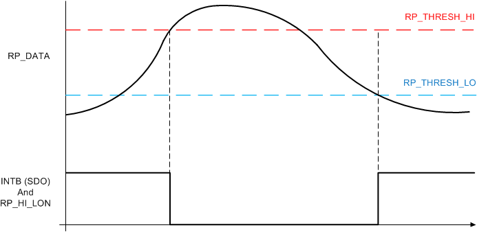 Figure 56. INTB/SDO Output Value for RP Comparator with Hysteresis (INTB_FUNC=b00’0010)
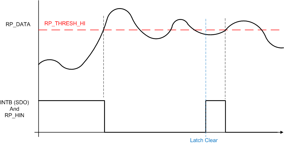 Figure 57. INTB/SDO Output for RP Threshold High (INTB_FUNC=b00’00011)
9.2 Typical Application
Implementation of a system using the LDC1101 first requires determining the appropriate measurement to perform. Refer to http://e2e.ti.com/blogs_/b/analogwire/archive/2015/02/11/inductive-sensing-should-i-measure-l-rp-or-both for guidance.
For systems that require measurement of RP, set the following:
- Configure RP settings as instructed in LDC1101 RP Configuration.
- Set the internal time constants as detailed in Setting Internal Time Constant 1 and Setting Internal Time Constant 2.
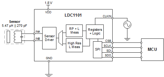 Figure 58. Example LDC1101 Typical Application
9.2.1 Design Requirements
Example of an axial measurement implementation using the LDC1101. In this example, the sensor is an inductor constructed of a multi-layer PCB coil in parallel with a C0G grade surface mount capacitor. For this example, a 10-mm diameter Aluminum target of 1mm thickness is moved perpendicular to the plane of the sensor coil.
For this example, the target range of motion is from 1-mm to 3-mm distance from the sensor coil. The position of the target needs to be reported at a sample rate of 3 ksps. The PCB is a 4-layer construction with 0.1-mm (4 mils) minimum feature size.
9.2.2 Detailed Design Procedure
9.2.2.1 Device Configuration for RP+L Measurement with an Example Sensor
The sensor described in Table 39 meets the restrictions on size on construction. To use it for RP+L measurement of a 10-mm diameter 1-mm thick aluminum target moving axially with respect to the sensor:
Table 39. Example Sensor Characteristics
| PARAMETER | MINIMUM TARGET INTERACTION | STRONGEST TARGET INTERACTION |
|---|---|---|
| Inductance | 5.47 µH | 5.15 µH |
| Inductor Outer Diameter | 10 mm | |
| Number of Turns | 17 | |
| Trace Spacing/ Trace Width | 0.1 mm / 0.16 mm | |
| Number of Layers/Separation | 2 / 0.355 mm | |
| Sensor Capacitance | 270 pF | |
| Sensor Frequency | 4.11 MHz | 4.27 MHz |
| RS | 3.2 Ω at 2.93 MHz | 3.23 Ω at 4.27 MHz |
| RP | 6.33 kΩ at 2.93 MHz | 5.91 kΩ at 4.27 MHz |
| Q at 2.9 MHz | 45 | 42 |
This sensor is within the LDC1101 sensor boundary conditions for frequency, Q, and RP. The first step is to determine the appropriate RPMIN/RPMAX and TC1/2 settings.
- Setting RPMAX has the constraint of RPD∞ ≤ RpMAX ≤ 2RPD∞
- RPMIN setting using the constraint of RpMIN < 0.8 × RPD0:
- Q Range: In step 4, the sensor Q range of 42 to 45 is within the operating range of 10 to 400. As the sensor Q value is below 50, it is not necessary to use HIGH_Q_SENSOR, and so HIGH_Q_SENSOR=0.
- Now set the Time Constant 1 using Equation 8:
- Next, set the Time Constant 2 using Equation 9:
- Then configure the MIN_FREQ field. The sensor minimum frequency is 4.11 MHz, which occurs with the minimum target interaction. Therefore, MIN_FREQ is set to 14, which configures the watchdog for 4.0 MHz.
- Next, set the response time. Setting 6144 provides the highest resolution RP measurement with this sensor. With 6144 the sample rate is at least 2.01 kSPS. To attain highest resolution with a sample rate of >3 kSPS, the response time setting should be 3072.
- All other device settings can be in their default values.
6.33 kΩ ≤ RPMAX ≤ 12.22 kΩ → Set RPMAX to 12 kΩ
0.8 × 3.20 kΩ = 2.6 kΩ → Set RPMIN to 1.5 kΩ. Therefore, set RPMIN = 1.5 kΩ.
R1 × C1 = 0.75026 ÷ 4.11 MHz = 1.8255E-7s
Starting with the largest C1 value of 6 pF for best noise performance results in R1 = 30.5 kΩ.
This is within the R1 range of 20.6 kΩ to 417.4 kΩ, and so C1 = 6 pF can be used.
Picking the next higher programmable value for R1 → Set R1 = 33.9 kΩ.
R2 × C2 = 2 × 1.5 kΩ × 270 pF = 8.100E-7s
Starting with the largest C2 value of 24 pF (once again, for best noise performance) results in
R2 = 33.75 kΩ.
This is within the programmable R2 value of 24.60 kΩ to 834.8 kΩ, and so 24 pF can be used for C2.
Picking the next higher programmable value for R2 → Set R2 = 43.3 kΩ.
Table 40. LDC1101 Register Settings for RP+L Example Application
| FIELD | FIELD SETTING | FIELD VALUE | REGISTER | REGISTER VALUE |
|---|---|---|---|---|
| HIGH_Q_SENSOR | disabled | b0 | RP_SET (0x01) | 0x36 |
| RPMAX | 12.0 kΩ | b011 | ||
| RPMIN | 1.5 kΩ | b110 | ||
| C1 | 6 pF | b11 | TC1 (0x02) | 0xDE |
| R1 | 33.9 kΩ | b1’1110 | ||
| C2 | 24 pF | b11 | TC2 (0x03) | 0xFE |
| R2 | 43.3 kΩ | b11’1110 | ||
| MIN_FREQ | 4.0 MHz | b1110 | DIG_CONF (0x04) | 0xE6 |
| RESP_TIME | 3072 | b110 | ||
| FUNC_MODE | active | b00 | START_CONFIG (0x0B) | 0x00 |
On power-up, the LDC1101 enters Sleep mode, which is a low power mode used to configure the LDC. If the LDC1101 is actively converting, write 0x01 to START_CONFIG (address 0x0B) to stop conversions before writing the settings above.
Once the LDC1101 is configured, the process to retrieve RP+L conversion results is:
- Set the LDC1101 into conversion mode (active mode) by writing 0x00 to START_CONFIG (register 0x0B).
- Poll STATUS.DRDYB (register 0x20:bit6) until it indicates a conversion result is present, or use the INTB signal reporting as described in DRDY (Data Ready) Reporting on SDO.
- If the desired measurement is RP, then read back registers 0x21 and 0x22. The RP output code is the contents of register 0x21 + 256 × (contents of register 0x22).
- If the desired measurement is L, then read back registers 0x23 and 0x24. The L output code is the contents of register 0x23 + 256 × (contents of register 0x24). Reading both RP and L is permitted, for a more efficient operation RP and L registers can be retrieved in a single extended SPI transaction as described in SPI Programming.
- Process the conversion results on the MCU and repeat from step 2 if additional conversions are desired. If no additional conversions are required, place the LDC1101 into Sleep mode or Shutdown mode.
9.2.2.2 Device Configuration for LHR Measurement with an Example Sensor
The LDC1101 can be configured for either RP and inductance (L) measurements or to only perform inductance (L) measurements. If the LDC1101 is to measure both RP and inductance, configure the RP measurement as described above. If only L measurements are needed, then configure the device for this operation as detailed in Setting RPMIN for LHR Measurements.
Given a sensor with characteristics as shown in Table 39, the steps to configure the LDC1101 for LHR measurements are:
- Determine the device sample rate, based on system requirements, using Equation 14. For this example, ƒCLKIN = 16 MHz and a sample rate of 3 kSPS is necessary. The number of cycles of the ƒCLKIN that closest fit the desired sample rate is determined by:
mm 1/(3 kSPS) = 333.3 µs
subtracting the conversion post-processing time of 55 reference clock cycles (55/16 MHz = 3.437 µs):
mm 333.3 µs – 3.437 µs = 329.9 µs → 16 MHz × 329.9 µs = 5278.33 → 5278.33/16 = 329.9
Programming RCOUNT to 330 (0x014A) results in a sample rate of 2.999 kSPS. - Next, set the sensor drive current. If the sensor was already configured for RP+L measurements with the steps in Device Configuration for RP+L Measurement with an Example Sensor, then the sensor drive is already configured and no additional steps are necessary.
- If the sensor drive current needs to be configured, from Table 36, 3 kΩ is the appropriate setting for the sensor RP range of 6.33 kΩ to 5.91 kΩ.
Table 41. LDC1101 Register Settings for LHR Example Application
Once the LDC1101 is configured, the process to retrieve LHR conversion results is:
- Set the LDC1101 into conversion mode (active mode) by writing 0x00 to START_CONFIG (register 0x0B).
- Poll LHR_STATUS.DRDYB (register 0x3B:bit0) until it indicates a conversion result is present, or use the INTB signal reporting as described in DRDY (Data Ready) Reporting on SDO.
- Read back registers 0x38, 0x39, and 0x3A. These registers can be retrieved in a single extended SPI transaction as described in SPI Programming.
- Process the conversion results on the MCU and repeat from step 2 if additional conversions are desired. If no additional conversions are required, place the LDC1101 into Sleep mode or Shutdown mode.
Both sets of conversion results can be retrieved when the conversions complete. Note that the RP+L conversions do not complete at the same time as LHR conversions.
9.2.3 Application Curves
The RCOUNT = 0x00FF curve, which corresponds to a sample rate of 3.87 ksps, measures the target position with a slightly lower resolution than the RCOUNT = 0x014A used in this example. Over the target movement range of 3 mm, which corresponds to the normalized value of 0.3 on the Axial Measurement graph, the target position can be resolved to 4 µm.
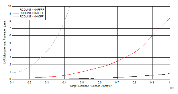 Figure 59. LHR Axial Measurement Resolution vs Normalized Distance for Aluminum Target
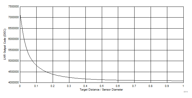 Figure 60. LHR Output Code vs Normalized Distance for Aluminum Target