SNOSD01D May 2015 – October 2016
PRODUCTION DATA.
- 1 Features
- 2 Applications
- 3 Description
- 4 Simplified Schematic
- 5 Revision History
- 6 Pin Configuration and Functions
- 7 Specifications
-
8 Detailed Description
- 8.1 Overview
- 8.2 Functional Block Diagram
- 8.3 Feature Description
- 8.4
Device Functional Modes
- 8.4.1 Measurement Modes
- 8.4.2 RP+L Measurement Mode
- 8.4.3 High Resolution L (LHR) Measurement Mode
- 8.4.4 Reference Count Setting
- 8.4.5 L-Only Measurement Operation
- 8.4.6 Minimum Sensor Frequency and Watchdog Setting
- 8.4.7 Low Power Modes
- 8.4.8 Status Reporting
- 8.4.9 Switch Functionality and INTB Reporting
- 8.5 Programming
- 8.6
Register Maps
- 8.6.1 Individual Register Listings
- 8.6.2 Register RP_SET (address = 0x01) [reset = 0x07]
- 8.6.3 Register TC1 (address = 0x02) [reset = 0x90]
- 8.6.4 Register TC2 (address = 0x03) [reset = 0xA0]
- 8.6.5 Register DIG_CONF (address = 0x04) [reset = 0x03]
- 8.6.6 Register ALT_CONFIG (address = 0x05) [reset = 0x00]
- 8.6.7 Register RP_THRESH_HI_LSB (address = 0x06) [reset = 0x00]
- 8.6.8 Register RP_THRESH_HI_MSB (address = 0x07) [reset = 0x00]
- 8.6.9 Register RP_THRESH_LO_LSB (address = 0x08) [reset = 0x00]
- 8.6.10 Register RP_THRESH_LO_MSB (address = 0x09) [reset = 0x00]
- 8.6.11 Register INTB_MODE (address = 0x0A) [reset = 0x00]
- 8.6.12 9.Register START_CONFIG (address = 0x0B) [reset = 0x01]
- 8.6.13 Register D_CONFIG (address = 0x0C) [reset = 0x00]
- 8.6.14 Register L_THRESH_HI_LSB (address = 0x16) [reset = 0x00]
- 8.6.15 Register L_THRESH_HI_MSB (address = 0x17) [reset = 0x00]
- 8.6.16 Register L_THRESH_LO_LSB (address = 0x18) [reset = 0x00]
- 8.6.17 Register L_THRESH_LO_MSB (address = 0x19) [reset = 0x00]
- 8.6.18 Register STATUS (address = 0x020 [reset = 0x00]
- 8.6.19 Register RP_DATA_LSB (address = 0x21) [reset = 0x00]
- 8.6.20 Register RP_DATA_MSB (address = 0x22) [reset = 0x00]
- 8.6.21 Register L_DATA_LSB (address = 0x23) [reset = 0x00]
- 8.6.22 Register L_DATA_MSB (address = 0x24) [reset = 0x00]
- 8.6.23 Register LHR_RCOUNT_LSB (address = 0x30) [reset = 0x00]
- 8.6.24 Register LHR_RCOUNT_MSB (address = 0x31) [reset = 0x00]
- 8.6.25 Register LHR_OFFSET_LSB (address = 0x32) [reset = 0x00]
- 8.6.26 Register LHR_OFFSET_MSB (address = 0x33) [reset = 0x00]
- 8.6.27 Register LHR_CONFIG (address = 0x34) [reset = 0x00]
- 8.6.28 Register LHR_DATA_LSB (address = 0x38) [reset = 0x00]
- 8.6.29 Register LHR_DATA_MID (address = 0x39) [reset = 0x00]
- 8.6.30 Register LHR_DATA_MSB (address = 0x3A) [reset = 0x00]
- 8.6.31 Register LHR_STATUS (address = 0x3B) [reset = 0x00]
- 8.6.32 Register RID (address = 0x3E) [reset = 0x02]
- 8.6.33 Register DEVICE_ID (address = 0x3F) [reset = 0xD4]
-
9 Application and Implementation
- 9.1
Application Information
- 9.1.1 TI Designs and Application Notes
- 9.1.2 Theory of Operation
- 9.1.3 RP+L Mode Calculations
- 9.1.4 LDC1101 RP Configuration
- 9.1.5 Setting Internal Time Constant 1
- 9.1.6 Setting Internal Time Constant 2
- 9.1.7 MIN_FREQ and Watchdog Configuration
- 9.1.8 RP+L Sample Rate Configuration With RESP_TIME
- 9.1.9 High Resolution Inductance Calculation (LHR mode)
- 9.1.10 LHR Sample Rate Configuration With RCOUNT
- 9.1.11 Setting RPMIN for LHR Measurements
- 9.1.12 Sensor Input Divider
- 9.1.13 Reference Clock Input
- 9.1.14 INTB Reporting on SDO
- 9.1.15 DRDY (Data Ready) Reporting on SDO
- 9.1.16 Comparator Functionality
- 9.2 Typical Application
- 9.1
Application Information
- 10Power Supply Recommendations
- 11Layout
- 12Device and Documentation Support
- 13Mechanical, Packaging, and Orderable Information
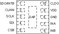
6 Pin Configuration and Functions
DRC Package
10-Pin VSON
Top View

Pin Functions
| PIN | TYPE(1) | DESCRIPTION | |
|---|---|---|---|
| NAME | NO. | ||
| CLDO | 10 | P | Internal LDO bypassing pin. A 15-nF capacitor must be connected from this pin to GND. |
| CLKIN | 2 | I | External time-base clock Input |
| CSB | 5 | I | SPI CSB. Multiple devices can be connected on the same SPI bus and CSB can be used to uniquely select desired device. CSB must be toggled for proper device operation. |
| DAP | – | – | Connect to ground for improved thermal performance(2) |
| GND | 8 | G | Ground |
| INA | 7 | A | External LC sensor – connect to external LC sensor |
| INB | 6 | A | External LC sensor – connect to external LC sensor |
| SCLK | 3 | I | SPI clock input |
| SDI | 4 | I | SPI data input – connect to MOSI of SPI master |
| SDO/INTB | 1 | O | SPI data output/INTB – Connect to MISO of SPI master. When CSB is high, this pin is High-Z. Alternatively, this pin can be configured to function as INTB |
| VDD | 9 | P | Power supply |
(1) P= Power, G=Ground, I=Input, O=Output, A=Analog
(2) There is an internal electrical connection between the exposed Die Attach Pad (DAP) and the GND pin of the device. Although the DAP can be left floating, for best performance the DAP must be connected to the same potential as the GND pin of the device. Do not use the DAP as the primary ground for the device. The device GND pin must always be connected to ground.