SNOSD74B May 2019 – January 2020 LMG1025-Q1
PRODUCTION DATA.
8.2.2.1 Handling Ground Bounce
For the best switching performance and gate loop with lowest parasitics, it is recommended to connect the ground return pin of LMG1025-Q1 as close as possible to the source of the low-side FET in a low inductance manner. However, doing so can cause the ground of LMG1025-Q1 to bounce relative to the system or controller ground and lead to erroneous switching logic on the input so as mis-turn on/off on the output.
First of all, LMG1025-Q1 has input hysteresis built into the input buffers to help counteract this effect. The maximum di/dt allowed to prevent the input voltage transient from exceeding the input hysteresis is given by Equation 1

where
- LRS is the inductance of the sense resistor,
- VHYST is the hysteresis of the input pin,
- and dis/dt is the maximum allowed current slew rate.
For an assumed shunt resistor parasitic inductance of 0.5 nH and a minimum hysteresis of 0.5 V, the maximum slew rate is 1 A/ns. Many applications would exhibit higher current slew rates, up to the 10 A/ns range, which would make this approach impractical. The stability of this approach can be improved by using the IN– input for the PWM signal and locally tying IN+ to VDD. By using the inverting input, the transient voltage applied to the input pin reinforces the PWM signal in a positive feedback loop. While this approach would reduce the probability of false pulses or oscillation, the transient spikes due to high di/dt may overly stress the inputs to the LMG1025-Q1. A current-limiting, 100 Ω resistor can be placed right before the IN– input to limit excessive current spikes in the device.
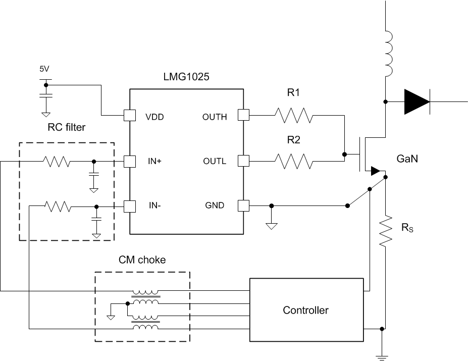
Secondly, for moderate ground-bounce cases, a simple R-C filter can be built with a simple resistor in series with the inputs. By utilizing the input capacitance of LMG1025-Q1, the resistor could be close to its input pin. The addition of a small capacitor on the input as supplement can also be helpful. A small time constant of the R-C filter may be enough to filter out high frequency noise. This solution is acceptable for moderate cases in applications where extra delay is acceptable and the pulse width is not extremely short such as in 1ns range.
For more extreme cases, or where no delay is tolerable while pulse width is extremely short, using a commonmode choke provides the best results.
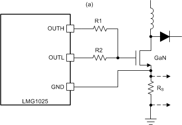
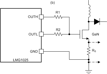
One example application where ground-bounce is particularly challenging is when using a current sense resistor. In Figure 7 LMG1025-Q1 ground is connected to the source of GaN FET, while the controller ground is connected to the other side of the current sense resistor as shown in Figure 7. Due to the fast switching and very fast current slew rates, the high ground potential bounce induced by inductance of the sense resistor can disrupt the operation of the circuit or even damage the part. To prevent this, a common-mode choke can be used for IN+ and IN–, respectively. Resistors can also added to the signal output line before LMG1025-Q1 depending on the input signal pulse width to provide additional RC filtering. Figure 9 presents the schematic using approach A with the preferred filtering method. Approach B as shown in Figure 8 places the current sense resistor within the gate drive loop path. In this case, the LMG1025-Q1 GND pin is connected to the signal ground, and with good ground plane connection, the ground bounce issue can be less severe than approach A. However, the inductance of the current sense resistor adds common-source inductance to the gate drive loop. The voltage generated across this parasitic inductance will subtract from the gate-drive voltage of the FET, slowing down the turnon and turnoff di/dt of the FET, or even cause mis-turn on and off. Additional gate resistance will have to be added to ensure the loop is stable and ring-free. The slower rise may negate the advantage of the fast switching of the GaN FET and may cause additional losses in the circuit. Therefore, this approach is not recommended.
 Figure 7. Source Resistor Current Sense A Configuration
  Figure 8. Source Resistor Current Sense B Configuration
  Figure 9. Filtering For Ground Bounce Noise Handling When Using LMG1025-Q1