SNOSD74B May   2019  – January 2020 LMG1025-Q1

PRODUCTION DATA.  

  1. Features
  2. Applications
  3. Description
    1.     Device Images
      1.      Typical (Simplified) System Diagram
  4. Revision History
  5. Pin Configuration and Functions
    1.     Pin Functions
  6. Specifications
    1. 6.1 Absolute Maximum Ratings
    2. 6.2 ESD Ratings
    3. 6.3 Recommended Operating Conditions
    4. 6.4 Thermal Information
    5. 6.5 Electrical Characteristics
    6. 6.6 Switching Characteristics
    7. 6.7 Typical Characteristics
  7. Detailed Description
    1. 7.1 Overview
    2. 7.2 Functional Block Diagram
    3. 7.3 Feature Description
      1. 7.3.1 Input Stage
      2. 7.3.2 Output Stage
      3. 7.3.3 Bias Supply and Under Voltage Lockout
      4. 7.3.4 Overtemperature Protection (OTP)
    4. 7.4 Device Functional Modes
  8. Application and Implementation
    1. 8.1 Application Information
    2. 8.2 Typical Application
      1. 8.2.1 Design Requirements
      2. 8.2.2 Detailed Design Procedure
        1. 8.2.2.1 Handling Ground Bounce
        2. 8.2.2.2 Creating Nanosecond Pulse
      3. 8.2.3 VDD and Overshoot
      4. 8.2.4 Operating at Higher Frequency
      5. 8.2.5 Application Curves
  9. Power Supply Recommendations
  10. 10Layout
    1. 10.1 Layout Guidelines
      1. 10.1.1 Gate Drive Loop Inductance and Ground Connection
      2. 10.1.2 Bypass Capacitor
    2. 10.2 Layout Example
  11. 11Device and Documentation Support
    1. 11.1 Receiving Notification of Documentation Updates
    2. 11.2 Support Resources
    3. 11.3 Trademarks
    4. 11.4 Electrostatic Discharge Caution
    5. 11.5 Glossary
  12. 12Mechanical, Packaging, and Orderable Information

Pin Configuration and Functions

DEE
6-Pin WSON
Top View
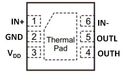
LMG1025-Q1 lotus-package.gif

Pin Functions

PIN I/O(1) DESCRIPTION
NAME NO.
GND 2 G Power supply and source return. Connect with a direct path to the transistor’s source.
IN+ 1 I Positive logic-level input.
IN– 6 I Negative logic-level input.
OUTL 5 O Pull-down gate drive output. Connect through an optional resistor to the target transistor’s gate.
OUTH 4 O Pull-up gate drive output. Connect through a resistor to the target transistor’s gate.
VDD 3 P Input voltage supply. Decouple through a compact capacitor to GND.
Thermal Pad - - Internally connected to GND through substrate. Connect this pad to large copper area, generally a ground plane.
I=Input, O=Output, P=Power, G=Ground