SNOU180A June 2021 – September 2021 LM74701-Q1
2.1 I/O Connector Description
-
VIN
J1: Power input connector to the positive rail
of the input power supply
-
GND1
J3: Ground connection for the power
supply
-
VOUT
J2: Power output connector to the positive
side of the load
-
GND2
J4: Ground connection for the load
-
EN
J5: Jumper to enable LM74701-Q1 gate driver
1-2 position connects EN to Anode, 2-3 position connects EN to GND
-
Test Points
VINA, VOUTA,GATE,ENA,BATT_MON, GND1, and GND2
are test points
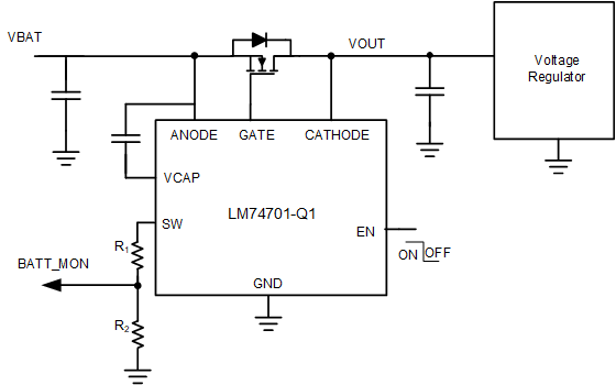
 Figure 2-1 LM74701-Q1EVM Typical Application
Circuit