SNVA067D April 2013 – August 2022 LM3478 , LM3481 , LM3488
2 Error Amplifier
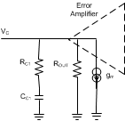
This completes the equation of the control to output transfer function. The second stage that needs to be analyzed is the error amplifier. Of particular interest, we will derive the transfer function from the feedback pin to the control voltage. To achieve this, the error amplifier block diagram has been converted to a small signal model.

As can be seen, the LM3478 uses a gm amplifier for the error amplifier. With this model the equation can be written by inspection as:

The DC gain of the system AEA is simply the output conductance multiplied by the output resistance of the amplifier. These values can be found in the electrical characteristics table of the datasheet.
The single zero is formed by the two external compensation components that are added at the COMP pin of the LM3478, the capacitor and resistor.

The error amplifier pole is formed by the combination of the output resistance of the error amplifier and the external compensation capacitor. An additional pole can be added with the introduction of another capacitor CC2 in parallel. However, for most power supplies this is not necessary.

The last transfer function that needs to be derived in the loop is from the output voltage, VOUT, to the feedback pin. This can be calculated by inspection and is simply a voltage divider, caused by the feedback resistors. This can be written as a combination of the resistors or the output voltage and feedback voltage for convenience
