SNVAA05 October 2020 LM60430-Q1 , LM60440-Q1
4 Pin Failure Mode Analysis (Pin FMA)
This section provides a Failure Mode Analysis (FMA) for the pins of the LM60430-Q1 and LM60440-Q1. The failure modes covered in this document include the typical pin-by-pin failure scenarios:
- Pin short-circuited to Ground (see Table 4-2)
- Pin open-circuited (see Table 4-3)
- Pin short-circuited to an adjacent pin (see Table 4-4)
- Pin short-circuited to input (see Table 4-5)
Table 4-2 through Table 4-5 also indicate how these pin conditions can affect the device as per the failure effects classification in Table 4-1.
| Class | Failure Effects |
|---|---|
| A | Potential device damage that affects functionality |
| B | No device damage, but loss of critical functionality |
| C | No device damage, but performance degradation |
| D | No device damage, no impact to functionality or performance |
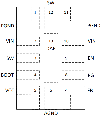
Figure 4-1 shows the LM60430-Q1 and LM60440-Q1 pin diagram. For a detailed description of the device pins please refer to the 'Pin Configuration and Functions' section in the LM60430-Q1 and LM60440-Q1 data sheet.
 Figure 4-1 Pin Diagram: LM60430-Q1,
LM60440-Q1
Figure 4-1 Pin Diagram: LM60430-Q1,
LM60440-Q1Following are the assumptions of use and the device configuration assumed for the pin FMA in this section:
| Pin Name | Pin No | Description of Potential Failure Effect(s) | Failure Effect Class |
|---|---|---|---|
| PGND | 1 | Normal Operation | D |
| VIN | 2,10 | Input supply would collapse and as a result there will be no output voltage | B |
| SW | 3,12 | Damage to power switches likely; loss of VOUT regulation | A |
| BOOT | 4 | No switching | B |
| VCC | 5 | No switching; loss of all functionality | B |
| AGND | 6 | Normal operation | D |
| FB | 7 | Loss of VOUT regulation | B |
| PG | 8 | Loss of power good indicator if used | C |
| EN | 9 | IC will not start | B |
| PGND | 11 | Normal operation | D |
| Pin Name | Pin No | Description of Potential Failure Effect(s) | Failure Effect Class |
|---|---|---|---|
| PGND | 1 | Vout normal; current distribution in power switched will be affected, potentially degrading jitter/EMI/reliability | C |
| VIN | 2,10 | Vout normal; current distribution in power switched will be affected, potentially degrading jitter/EMI/reliability | C |
| SW | 3 | Loss of VOUT regulation | B |
| BOOT | 4 | No switching | B |
| VCC | 5 | Internal VCC supply will be unstable without VCC bypass capacitor; abs max maybe exceeded; possibly loss of VOUT regulation | A |
| AGND | 6 | May increase noise/jitter and possibly loss of regulation | B |
| FB | 7 | Loss of VOUT regulation | B |
| PG | 8 | Loss of power good indicator if used | C |
| EN | 9 | Possible loss of VOUT regulation | B |
| PGND | 11 | Vout normal; current distribution in power switched will be affected, potentially degrading jitter/EMI/reliabilit | C |
| SW | 12 | No switching, if CB returns via this pin | B |
| Pin Name | Pin No | Description of Potential Failure Effect(s) | Failure Effect Class |
|---|---|---|---|
| PGND | 1 | Input supply would collapse and as a result there will be no output voltage | B |
| VIN | 2 | Damage to power siwtches likely; loss of VOUT regulation | A |
| SW | 3 | Loss of VOUT regulation | B |
| BOOT | 4 | No switching | B |
| VCC | 5 | No switching; loss of all functionality | B |
| AGND | 6 | Loss of VOUT regulation | B |
| FB | 7 | Abs max may be exceeded, and loss of VOUT regulation | A |
| PG | 8 | Abs max may be exceeded, and possibly unable to start | A |
| EN | 9 | Normal operation; IC will not shut down | C |
| VIN | 10 | Input supply would collapse and as a result there will be no output voltage | B |
| PGND | 11 | Damage to the power switches likely; loss of VOUT regulation | A |
| SW | 12 | Damage to the power switches likely; loss of VOUT regulation | A |
| Pin Name | Pin No | Description of Potential Failure Effect(s) | Failure Effect Class |
|---|---|---|---|
| PGND | 1 | Input supply would collapse and as a result there will be no output voltage | B |
| VIN | 2,10 | Normal operation | D |
| SW | 3,12 | Damage to the power switches likely; loss of VOUT regulation | A |
| BOOT | 4 | Damage to the driver circuitry likely; loss of VOUT regulation | A |
| VCC | 5 | Abs max may be exceeded | A |
| AGND | 6 | Input supply would collapse and as a result there will be no output voltage | B |
| FB | 7 | Abs max may be exceeded; loss of VOUT regulation | A |
| PG | 8 | Abs max may be exceeded | A |
| EN | 9 | Normal operation; IC will not shut off | C |
| PGND | 11 | Input supply would collapse and as a result there will be no output voltage | B |