SNVS358R July 2005 – June 2016 LP5900
PRODUCTION DATA.
7 Detailed Description
7.1 Overview
Designed to meet the needs of sensitive RF and analog circuits, the LP5900 provides low noise, high PSRR, and low quiescent current, as well as low line and load transient response figures. Using new innovative design techniques, the LP5900 offers class-leading noise performance without the need for a separate noise filter capacitor.
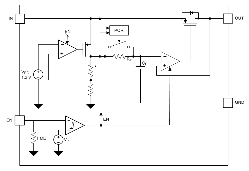
7.2 Functional Block Diagram

7.3 Feature Description
7.3.1 No-Load Stability
The LP5900 remains stable and in regulation with no external load.
7.3.2 Enable Control
The LP5900 enable (EN) pin is internally held low by a 1-MΩ resistor to GND. The EN must be higher than the VIH threshold to ensure that the device is fully enabled under all operating conditions. The EN pin voltage must be lower than the VIL threshold to ensure that the device is fully disabled.
7.3.3 Low Noise Output
Any internal noise at the LP5900 reference voltage is reduced by a first order low-pass RC filter before it is passed to the output buffer stage. This eliminates the need for the external bypass capacitor for noise suppression.
7.3.4 Thermal-Overload Protection
Thermal-overload protection disables the output when the junction temperature rises to approximately 160°C which allows the device to cool. When the junction temperature cools to approximately 140°C, the output is enabled. Based on power dissipation, thermal resistance, and ambient temperature, the thermal protection circuit may cycle on and off. This thermal cycling limits the dissipation of the regulator and protects it from damage as a result of overheating.
7.4 Device Functional Modes
7.4.1 Operation with Enable Control
The LP5900 may be switched ON or OFF by a logic input at the EN pin. A high voltage at this pin turns the device on. When the EN pin is low, the regulator output is off, and the device typically consumes 3 nA. However, if the application does not require the shutdown feature, the EN pin can be tied to IN pin to keep the regulator output permanently on. In this case the supply voltage must be fully established 500 μs or less to ensure correct operation of the start-up circuit. Failure to comply with this condition may cause a delayed start-up time of several seconds.
A 1 MΩ pull-down resistor ties the EN input to ground, and this ensures that the device will remain off when the EN pin is left open circuit. To ensure proper operation, the signal source used to drive the EN input must be able to swing above and below the specified turn-on/off voltage thresholds listed in the Electrical Characteristics section under VIL and VIH.
7.4.2 Operation with Minimum Operating Input Voltage (VIN)
The LP5900 does not include any dedicated UVLO circuitry. The LP5900 internal circuitry is not fully functional until VIN is at least 2.5 V. The output voltage is not regulated until VIN ≥ (VOUT + VDO).