SNVS550E September 2009 – January 2017 LP5523
PRODUCTION DATA.
- 1 Features
- 2 Applications
- 3 Description
- 4 Revision History
- 5 Pin Configuration and Functions
-
6 Specifications
- 6.1 Absolute Maximum Ratings
- 6.2 ESD Ratings
- 6.3 Recommended Operating Conditions
- 6.4 Thermal Information
- 6.5 Electrical Characteristics
- 6.6 Charge Pump Electrical Characteristics
- 6.7 LED Driver Electrical Characteristics
- 6.8 LED Test Electrical Characteristics
- 6.9 Logic Interface Characteristics
- 6.10 Recommended External Clock Source Conditions
- 6.11 Serial Bus Timing Parameters (SDA, SCL)
- 6.12 Typical Characteristics
-
7 Detailed Description
- 7.1 Overview
- 7.2 Functional Block Diagram
- 7.3 Feature Description
- 7.4 Device Functional Modes
- 7.5 Programming
- 7.6 Register Maps
- 8 Application and Implementation
- 9 Power Supply Recommendations
- 10Layout
- 11Device and Documentation Support
- 12Mechanical, Packaging, and Orderable Information
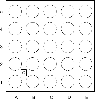
5 Pin Configuration and Functions
YFQ Package
25-Pin DSBGA
Top View

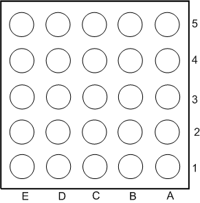
YFQ Package
25-Pin DSBGA
Bottom View

Pin Functions(1)
| PIN | TYPE | DESCRIPTION | |
|---|---|---|---|
| NO. | NAME | ||
| A1 | D1 | A | Current source output 1 |
| A2 | D2 | A | Current source output 2 |
| A3 | VOUT | A | Charge pump output |
| A4 | C2− | A | Flying capacitor 2 negative terminal |
| A5 | C2+ | A | Flying capacitor 2 positive terminal |
| B1 | D3 | A | Current source output 3 |
| B2 | D4 | A | Current source output 4 |
| B3 | ASEL1 | I | Serial interface address select input |
| B4 | C1− | A | Flying capacitor 1 negative terminal |
| B5 | C1+ | A | Flying capacitor 1 positive terminal |
| C1 | D5 | A | Current source output 5 |
| C2 | D6 | A | Current source output 6 |
| C3 | ASEL0 | I | Serial interface address select input |
| C4 | EN | I | Enable |
| C5 | VDD | P | Input power supply |
| D1 | D7 | A | Current source output 7 - powered from VDD |
| D2 | D8 | A | Current source output 8 - powered from VDD |
| D3 | INT | OD/O | Interrupt for microcontroller unit. Leave unconnected if not used |
| D4 | CLK | I | 32 kHz clock input. Connect to ground if not used |
| D5 | GND | G | Ground |
| E1 | D9 | A | Current source output 9 - powered from VDD |
| E2 | GPO | O | General purpose output. Leave unconnected if not used |
| E3 | TRIG | I/OD | Trigger. Connect to ground if not used. |
| E4 | SDA | I/OD | Serial interface data |
| E5 | SCL | I | Serial interface clock |
(1) A: Analog Pin G: Ground Pin P: Power Pin I: Input Pin I/O: Input/Output Pin O: Output Pin OD: Open Drain Pin