SNVS820B APRIL 2013 – December 2016
PRODUCTION DATA.
- 1 Features
- 2 Applications
- 3 Description
- 4 Revision History
- 5 Pin Configuration and Functions
-
6 Specifications
- 6.1 Absolute Maximum Ratings
- 6.2 ESD Ratings
- 6.3 Recommended Operating Conditions
- 6.4 Thermal Information
- 6.5 Electrical Characteristics
- 6.6 Logic Interface Characteristics
- 6.7 Recommended External Clock Source Conditions
- 6.8 I2C Timing Requirements (SDA, SCL)
- 6.9 Typical Characteristics: Current Consumption
- 6.10 Typical Characteristics: LED Output
-
7 Detailed Description
- 7.1 Overview
- 7.2 Functional Block Diagram
- 7.3
Feature Description
- 7.3.1 LED Drivers Operational Description
- 7.3.2 Direct I2C Register PWM Control Example
- 7.3.3 Program Execution Engines
- 7.3.4 Power-Save Mode
- 7.3.5 External Clock
- 7.3.6 Thermal Shutdown
- 7.3.7 Logic Interface Operational Description
- 7.3.8 I/O Levels
- 7.3.9 ADDR_SEL0, ADDR_SEL1 Pins
- 7.3.10 CLK_32 Pin
- 7.4 Device Functional Modes
- 7.5 Programming
- 7.6
Register Maps
- 7.6.1 Enable Register (Enable) (Address = 00h) [reset = 00h]
- 7.6.2 Operation Mode Register (OP Mode) (address = 01h) [reset = 00h]
- 7.6.3 B LED Output PWM Control Register (B_PWM) (address = 02h) [reset = 00h]
- 7.6.4 G LED Output PWM Control Register (G_PWM) (address = 03h) [reset = 00h]
- 7.6.5 R LED Output PWM Control Register (R_PWM) (address = 04h) [reset = 00h]
- 7.6.6 B LED Output Current Control Register (B_CURRENT)(address = 05h) [reset = AFh]
- 7.6.7 G LED Output Current Control Register (G_CURRENT)(address = 06h) [reset = AFh]
- 7.6.8 R LED Output Current Control Register (R_CURRENT) (address = 07h) [reset = AFh]
- 7.6.9 Configuration Control Register (CONFIG) (address = 08h) [reset = 00h]
- 7.6.10 Engine 1 Program Counter Value Register (Engine 1 PC) (address = 09h) [reset = 00h]
- 7.6.11 Engine 2 Program Counter Value Register (Engine 2 PC) (address = 0Ah) [reset = 00h]
- 7.6.12 Engine 3 Program Counter Value Register (Engine 3 PC) (address = 0Ah) [reset = 00h]
- 7.6.13 STATUS/INTERRUPT Register (address = 0Ch) [reset = 00h]
- 7.6.14 RESET Register (address = 0Dh) [reset = 00h]
- 7.6.15 WLED Output PWM Control Register (W_PWM) (address = 0Eh) [reset = 00h]
- 7.6.16 W LED Output Current Control Register (W_CURRENT) (address = 0Fh) [reset = AFh]
- 7.6.17 LED Mapping Register (LED Map) (address = 70h) [reset = 39h]
- 7.6.18 Program Memory (address = 10h - 6Fh) [reset = 00h]
- 8 Application and Implementation
- 9 Power Supply Recommendation
- 10Layout
- 11Device and Documentation Support
- 12Mechanical, Packaging, and Orderable Information
8 Application and Implementation
NOTE
Information in the following applications sections is not part of the TI component specification, and TI does not warrant its accuracy or completeness. TI’s customers are responsible for determining suitability of components for their purposes. Customers should validate and test their design implementation to confirm system functionality.
8.1 Application Information
The LP5562 is designed for mobile applications with an input voltage VIN between 2.7 V to 5.5 V to support a 1S lithium-ion battery source. A microcontroller or other I2C host is required to initialize and configure the LP5562 after power-up. An internal of external 32-kHz clock is required. If multiple LP5562 devices are used to sequence multiple RGB LEDs, then the external 32-kHz clock input is required. The ADDRSEL0 and ADDRSEL1 pins can be used to allow unique sequencing of up to four LP5562 devices on the same I2C bus.
The four LED current drivers can be configured up to 25.5-mA LED current each and are tolerant up to 6-V LED supply voltage.
8.2 Typical Application
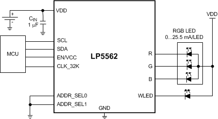
Figure 44 shows the typical application for LP5562 supporting one RGB LED and one White LED with the four LED current outputs.
 Figure 44. LP5562 Typical Application
8.2.1 Design Requirements
For typical LED-driver applications, use the parameters listed in Table 44.
Table 44. Design Parameters
| DESIGN PARAMETER | EXAMPLE VALUE |
|---|---|
| Minimum input voltage | 2.7 V |
| Maximum input voltage | 5.5 V |
| EN/VCC logic level | 1.8 V |
| R output current | 24 mA |
| G output current | 20 mA |
| B output current | 22 mA |
| WLED output current | 18 mA |
| PWM frequency | 256 Hz |
| 32-kHz clock source | External |
| Light engines 1, 2 and 3 | Blink on/off |
| Power-save mode | Enabled |
8.2.2 Detailed Design Procedure
Table 45. Recommended External Components
| MODEL | TYPE | VENDOR | VOLTAGE RATING | SIZE INCH (MM) |
|---|---|---|---|---|
| 1 µF for CIN | ||||
| C1005X5R1A105K | Ceramic X5R | TDK | 10 V | 0402 (1005) |
| GRM155R61A105KE15D | Ceramic X5R | Murata | 10 V | 0402 (1005) |
| LEDs | User Defined | |||
8.2.2.1 Output Current Configuration
- For 22-mA “B” output current the register address 0x05 is set to 0xDC. B_CURRENT[7:0] = (22 mA / 0.1) = 220 decimal.
- For 22-mA “G” output current the register address 0x06 is set to 0xC8. G_CURRENT[7:0] = (20 mA / 0.1) = 200 decimal.
- For 24-mA “R” output current the register address 0x07 is set to 0xF0. R_CURRENT[7:0] = (24 mA / 0.1) = 240 decimal.
- For 18-mA “WLED” output current the register address 0x0F is set to 0xB4. W_CURRENT[7:0] = (18 mA / 0.1) = 180 decimal.
8.2.2.2 PWM Frequency Configuration
To set the PWM frequency to 256 Hz the PWM_HF bit must be written to '0'. It is located at register address 0x08 bit 6.
8.2.2.3 Clock Source Configuration
To set the clock source to external clock input the INT_CLK_EN and CLK_DET_EN bits are set to “00”. These are located at register address 0x08 bits 0 and 1.
8.2.2.4 Power-Save Mode Configuration
To enable the power save mode function the PWRSAVE_EN bit must be set to '1'. It is located at register address 0x08 bit 5.
8.2.2.5 Light Engine Configuration
Sample code for 100% to 0% duty blinking LED function is shown in Table 46.
Table 46. LED Function Sample Codes
| ADDRESS | VALUE | COMMENTS | |
|---|---|---|---|
| Engine 1 Section Start | |||
| 0 | 40FF | Loop1 | set_pwm 255 |
| 1 | 4D00 | wait 200 | |
| 2 | 4000 | set_pwm 0 | |
| 3 | 6000 | wait 500 | |
| 4 | A200 | branch 4, loop1 | |
| 5 | D000 | end, i | |
| Engine 2 Section Start | |||
| 10 | 40FF | Loop2 | set_pwm 255 |
| 11 | 4D00 | wait 200 | |
| 12 | 4000 | set_pwm 0 | |
| 13 | 6000 | wait 500 | |
| 14 | A290 | branch 5, loop2 | |
| 15 | D000 | end, i | |
| Engine 3 Section Start | |||
| 20 | 40FF | Loop3 | set_pwm 255 |
| 21 | 4D00 | wait 200 | |
| 22 | 4000 | set_pwm 0 | |
| 23 | 6000 | wait 500 | |
| 24 | A320 | branch 6, loop3 | |
| 25 | D000 | end, i | |
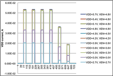
8.2.3 Application Curve

| External Clock | PS. Blink-Program | |