SNVS820B APRIL 2013 – December 2016
PRODUCTION DATA.
- 1 Features
- 2 Applications
- 3 Description
- 4 Revision History
- 5 Pin Configuration and Functions
-
6 Specifications
- 6.1 Absolute Maximum Ratings
- 6.2 ESD Ratings
- 6.3 Recommended Operating Conditions
- 6.4 Thermal Information
- 6.5 Electrical Characteristics
- 6.6 Logic Interface Characteristics
- 6.7 Recommended External Clock Source Conditions
- 6.8 I2C Timing Requirements (SDA, SCL)
- 6.9 Typical Characteristics: Current Consumption
- 6.10 Typical Characteristics: LED Output
-
7 Detailed Description
- 7.1 Overview
- 7.2 Functional Block Diagram
- 7.3
Feature Description
- 7.3.1 LED Drivers Operational Description
- 7.3.2 Direct I2C Register PWM Control Example
- 7.3.3 Program Execution Engines
- 7.3.4 Power-Save Mode
- 7.3.5 External Clock
- 7.3.6 Thermal Shutdown
- 7.3.7 Logic Interface Operational Description
- 7.3.8 I/O Levels
- 7.3.9 ADDR_SEL0, ADDR_SEL1 Pins
- 7.3.10 CLK_32 Pin
- 7.4 Device Functional Modes
- 7.5 Programming
- 7.6
Register Maps
- 7.6.1 Enable Register (Enable) (Address = 00h) [reset = 00h]
- 7.6.2 Operation Mode Register (OP Mode) (address = 01h) [reset = 00h]
- 7.6.3 B LED Output PWM Control Register (B_PWM) (address = 02h) [reset = 00h]
- 7.6.4 G LED Output PWM Control Register (G_PWM) (address = 03h) [reset = 00h]
- 7.6.5 R LED Output PWM Control Register (R_PWM) (address = 04h) [reset = 00h]
- 7.6.6 B LED Output Current Control Register (B_CURRENT)(address = 05h) [reset = AFh]
- 7.6.7 G LED Output Current Control Register (G_CURRENT)(address = 06h) [reset = AFh]
- 7.6.8 R LED Output Current Control Register (R_CURRENT) (address = 07h) [reset = AFh]
- 7.6.9 Configuration Control Register (CONFIG) (address = 08h) [reset = 00h]
- 7.6.10 Engine 1 Program Counter Value Register (Engine 1 PC) (address = 09h) [reset = 00h]
- 7.6.11 Engine 2 Program Counter Value Register (Engine 2 PC) (address = 0Ah) [reset = 00h]
- 7.6.12 Engine 3 Program Counter Value Register (Engine 3 PC) (address = 0Ah) [reset = 00h]
- 7.6.13 STATUS/INTERRUPT Register (address = 0Ch) [reset = 00h]
- 7.6.14 RESET Register (address = 0Dh) [reset = 00h]
- 7.6.15 WLED Output PWM Control Register (W_PWM) (address = 0Eh) [reset = 00h]
- 7.6.16 W LED Output Current Control Register (W_CURRENT) (address = 0Fh) [reset = AFh]
- 7.6.17 LED Mapping Register (LED Map) (address = 70h) [reset = 39h]
- 7.6.18 Program Memory (address = 10h - 6Fh) [reset = 00h]
- 8 Application and Implementation
- 9 Power Supply Recommendation
- 10Layout
- 11Device and Documentation Support
- 12Mechanical, Packaging, and Orderable Information
10 Layout
10.1 Layout Guidelines
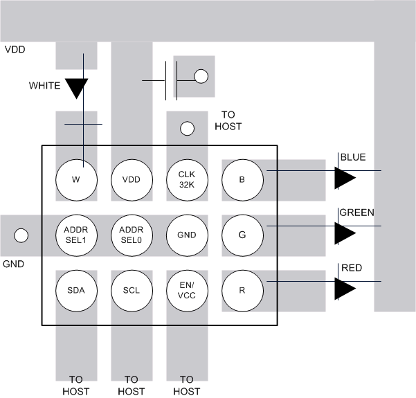
Figure 46 is a layout recommendation for the LP5562 used to demonstrate the principles of good layout. This example is for a 2-layer PCB and a single LP5562 device. This layout can be adapted to the actual application layout if/where possible. If multiple LP5562 devices are used in the application then not all the ADDRSEL pins will be tied to ground. In that case a PCB using HDI process is needed to route ADDRSEL0 and GND bumps. The VDD decoupling cap must be placed close to VDD bump, and the traces for W, R, G, and B bumps must be sized to carry 25.5 mA.
10.2 Layout Example
 Figure 46. LP5562 Layout Example