SNVSB03D December 2018 – January 2020
PRODUCTION DATA.
- 1 Features
- 2 Applications
- 3 Description
- 4 Revision History
- 5 Device Comparison
- 6 Pin Configuration and Functions
- 7 Specifications
- 8 Detailed Description
-
9 Application and Implementation
- 9.1 Application Information
- 9.2 Typical Application
- 10Power Supply Recommendations
- 11Layout
- 12Device and Documentation Support
- 13Mechanical, Packaging, and Orderable Information
6 Pin Configuration and Functions
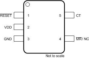
DBV Package
5-Pin SOT-23
TPS3840PL, TPS3840DL Top View
 Figure 2. Pin Configuration TPS3840PL, TPS3840DL
 DBV Package
5-Pin SOT-23
TPS3840PH Top View
 Figure 3. Pin Configuration TPS3840PH
 Pin Functions
| PIN | I/O | DESCRIPTION | ||
|---|---|---|---|---|
| NAME | TPS3840PL, TPS3840DL | TPS3840PH | ||
| RESET | N/A | 1 | O | Active-High Output Reset Signal: This pin is asserted to logic high when either the MR pin is pulled to a logic low or VDD voltage falls below the negative voltage threshold (VIT-). When both MR is floating or above VMR_H and VDD voltage rises above VIT+, RESET remains asserted to logic high (asserted) for the reset time delay (tD) before releasing back to logic low. |
| RESET | 1 | N/A | O | Active-Low Output Reset Signal: This pin is asserted to logic low when either the MR pin is pulled to a logic low or the VDD voltage falls below the negative voltage threshold (VIT-). When both MR is floating or above VMR_H and VDD voltage rises above VIT+, RESET remains asserted to logic low for the reset time delay (tD) before releasing back to logic high. |
| VDD | 2 | 2 | I | Input Supply Voltage. TPS3840 monitors VDD voltage |
| GND | 3 | 3 | _ | Ground |
| MR / NC | 4 | 4 | I | Manual Reset. Pull this pin to a logic low (VMR_L) to assert a reset signal at the RESET/RESET pin. If the MR pin is left floating or pulled to VMR_H, the output releases to the nominal state after the reset time delay (tD) expires. MR can be left floating when not in use. NC stands for "No Connection" or floating. |
| CT | 5 | 5 | - | Capacitor Time Delay Pin. The CT pin offers a user-programmable reset delay time. Connect an external capacitor on this pin to adjust the reset time delay. When not in use, leave pin floating for the smallest fixed reset time delay. |