SNVSB23 March 2018 LP87521-Q1 , LP87522-Q1 , LP87523-Q1 , LP87524-Q1 , LP87525-Q1
PRODUCTION DATA.
- 1 Features
- 2 Applications
- 3 Description
- 4 Revision History
- 5 Device Comparison Table
- 6 Pin Configuration and Functions
- 7 Specifications
-
8 Detailed Description
- 8.1 Overview
- 8.2 Functional Block Diagram
- 8.3
Feature Descriptions
- 8.3.1 Multi-Phase DC/DC Converters
- 8.3.2 Sync Clock Functionality
- 8.3.3 Power-Up
- 8.3.4 Regulator Control
- 8.3.5 Enable and Disable Sequences
- 8.3.6 Device Reset Scenarios
- 8.3.7 Diagnosis and Protection Features
- 8.3.8 GPIO Signal Operation
- 8.3.9 Digital Signal Filtering
- 8.4 Device Functional Modes
- 8.5 Programming
- 8.6
Register Maps
- 8.6.1
Register Descriptions
- 8.6.1.1 OTP_REV
- 8.6.1.2 BUCK0_CTRL1
- 8.6.1.3 BUCK1_CTRL1
- 8.6.1.4 BUCK2_CTRL1
- 8.6.1.5 BUCK3_CTRL1
- 8.6.1.6 BUCK0_VOUT
- 8.6.1.7 BUCK0_FLOOR_VOUT
- 8.6.1.8 BUCK1_VOUT
- 8.6.1.9 BUCK1_FLOOR_VOUT
- 8.6.1.10 BUCK2_VOUT
- 8.6.1.11 BUCK2_FLOOR_VOUT
- 8.6.1.12 BUCK3_VOUT
- 8.6.1.13 BUCK3_FLOOR_VOUT
- 8.6.1.14 BUCK0_DELAY
- 8.6.1.15 BUCK1_DELAY
- 8.6.1.16 BUCK2_DELAY
- 8.6.1.17 BUCK3_DELAY
- 8.6.1.18 GPIO2_DELAY
- 8.6.1.19 GPIO3_DELAY
- 8.6.1.20 RESET
- 8.6.1.21 CONFIG
- 8.6.1.22 INT_TOP1
- 8.6.1.23 INT_TOP2
- 8.6.1.24 INT_BUCK_0_1
- 8.6.1.25 INT_BUCK_2_3
- 8.6.1.26 TOP_STAT
- 8.6.1.27 BUCK_0_1_STAT
- 8.6.1.28 BUCK_2_3_STAT
- 8.6.1.29 TOP_MASK1
- 8.6.1.30 TOP_MASK2
- 8.6.1.31 BUCK_0_1_MASK
- 8.6.1.32 BUCK_2_3_MASK
- 8.6.1.33 SEL_I_LOAD
- 8.6.1.34 I_LOAD_2
- 8.6.1.35 I_LOAD_1
- 8.6.1.36 PGOOD_CTRL1
- 8.6.1.37 PGOOD_CTRL2
- 8.6.1.38 PGOOD_FLT
- 8.6.1.39 PLL_CTRL
- 8.6.1.40 PIN_FUNCTION
- 8.6.1.41 GPIO_CONFIG
- 8.6.1.42 GPIO_IN
- 8.6.1.43 GPIO_OUT
- 8.6.1
Register Descriptions
- 9 Application and Implementation
- 10Power Supply Recommendations
- 11Layout
- 12Device and Documentation Support
- 13Mechanical, Packaging, and Orderable Information
8.3.1.1 Overview
The LP8752x-Q1 includes four step-down DC/DC converter cores which can be configured for:
- 4-phase single output
- 3-phase and single-phase outputs
- dual-phase and two single-phase outputs
- four single-phase outputs
- two dual-phase outputs
The LP8752x-Q1 has the following features:
- DVS support
- Automatic mode control based on the loading (PFM or PWM mode)
- Forced-PWM mode operation
- Optional external clock input to minimize crosstalk
- Optional spread spectrum technique to decrease EMI
- Phase control for optimized EMI
- Synchronous rectification
- Current mode loop with PI compensator
- Soft start
- Power-Good flag with maskable interrupt
- Power-Good signal (PGOOD) with selectable sources
- Average output current sensing (for PFM entry, phase shedding/adding, and load current measurement)
- Current balancing between the phases of the converter
- Differential voltage sensing from point of the load for multiphase output
- Dynamic phase shedding/adding, each output being phase shifted
The following parameters can be programmed via registers:
- Output voltage
- Forced-PWM operation
- Forced multiphase operation for multiphase outputs (forces also the PWM operation)
- Enable and disable delays for regulators and GPIOs controlled by ENx pins
There are two modes of operation for the converter, depending on the output current required: pulse-width modulation (PWM) and pulse-frequency modulation (PFM). The converter operates in PWM mode at high load currents of approximately 600 mA or higher. When operating in PWM mode the phases of a multiphase regulator are automatically added/shedded based on the load current level. Lighter output current loads cause the converter to automatically switch into PFM mode for decreased current consumption when forced-PWM mode is disabled. The forced multiphase mode can be enabled for highest transient performance.
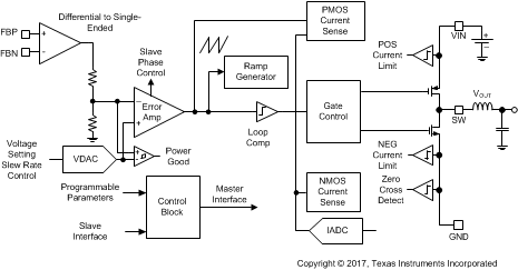
A multiphase synchronous buck converter offers several advantages over one power stage converter. For application processor power delivery, lower ripple on the input and output currents and faster transient response to load steps are the most significant advantages. Also, because the load current is evenly shared among multiple channels in multiphase output configuration, the heat generated is greatly decreased for each channel due to the fact that power loss is proportional to square of current. The physical size of the output inductor shrinks significantly due to this heat reduction. Figure 9 shows a block diagram of a single core.
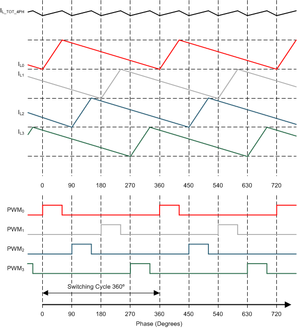
Interleaving switching action of the multiphase converters is shown in Figure 10.
 Figure 9. Detailed Block Diagram Showing One Core