SNVU658B March 2020 – May 2021 TPS54J060 , TPS54J061
- Trademarks
- 1Introduction
-
2Test Setup and Results
- 2.1 Input/Output Connections
- 2.2 Start Up Procedure
- 2.3 Efficiency
- 2.4 Load and Line Regulation
- 2.5 Load Transients
- 2.6 Loop Characteristics
- 2.7 Output Voltage Ripple
- 2.8 Input Voltage Ripple
- 2.9 Powering Up and Down with EN
- 2.10 Powering Up and Down With VIN
- 2.11 Start-Up Into Pre-Bias
- 2.12 Current Limit
- 3Schematic, List of Materials, and Layout
- Revision History
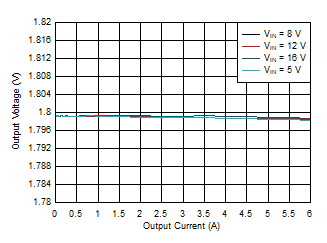
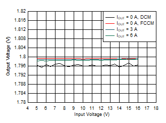
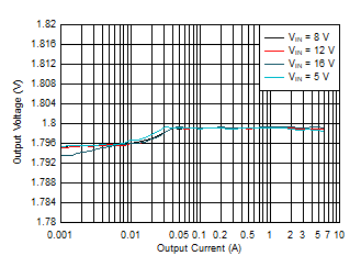
2.4 Load and Line Regulation
Figure 2-9 and Figure 2-10 shows the load regulation measured on the TPS54J060EVM-067. The output voltage of the TPS54J061EVM-067 is only slightly higher at 1.81V typical due to the different feedback divider.
 Figure 2-9 Load Regulation – FCCM
 Figure 2-11 Line Regulation
 Figure 2-10 Load Regulation – DCM