SNVU751 October   2020 LP875761-Q1


  1. 1Trademarks
  2. 2Overview
  3. 3Quick Setup Guide
    1. 3.1 Installing/Opening the Software
    2.     5
    3. 3.2 Power Supply Setup
    4. 3.3 Notes on Efficiency Measurement Procedure
  4. 4GUI Overview
    1. 4.1 Main Tab
    2. 4.2 Other Tabs and Menus
    3. 4.3 Console
  5. 5Bill of Materials
  6. 6Board Layout
  7. 7LP875761Q1EVM Schematics
  8. 8Revision History

Board Layout

This section describes the board layout of the LP875761Q1EVM. See the LP875761-Q1 data sheet for specific PCB layout recommendations.

The board is constructed on a 4-layer PCB. using 55-µm copper on top and bottom layers to reduce resistance and improve heat transfer.

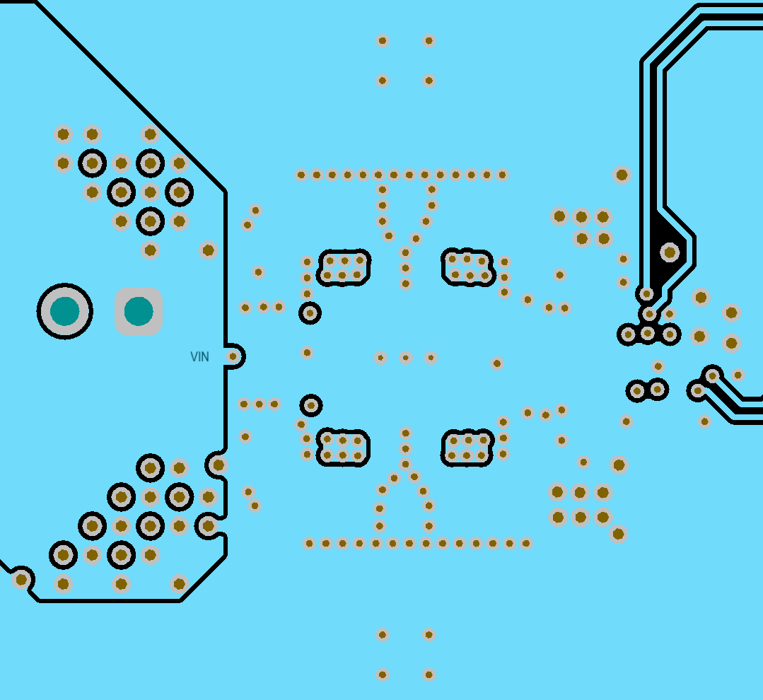
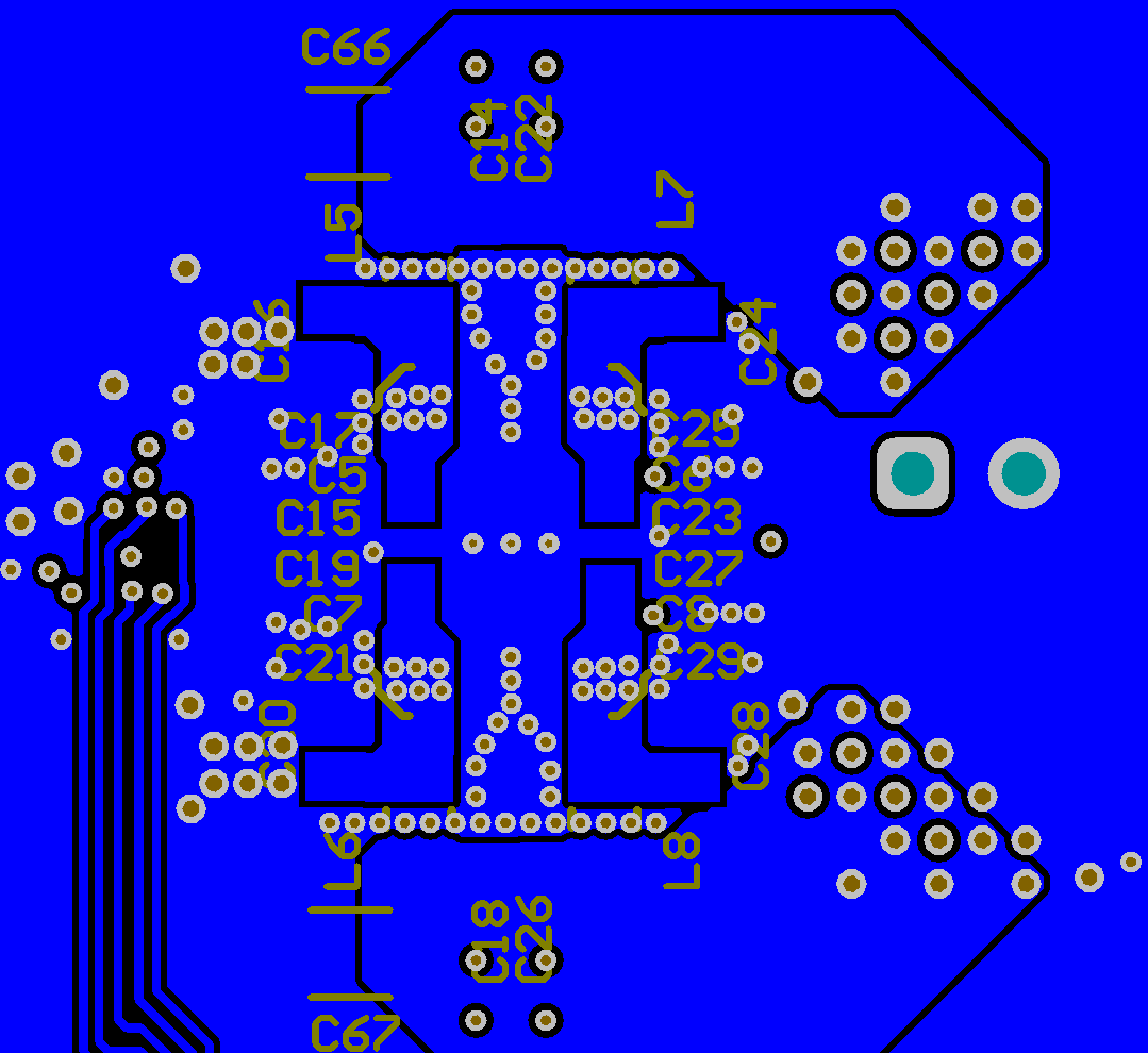
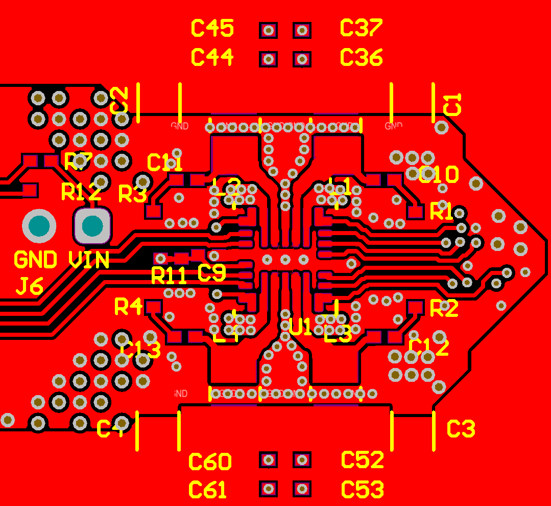
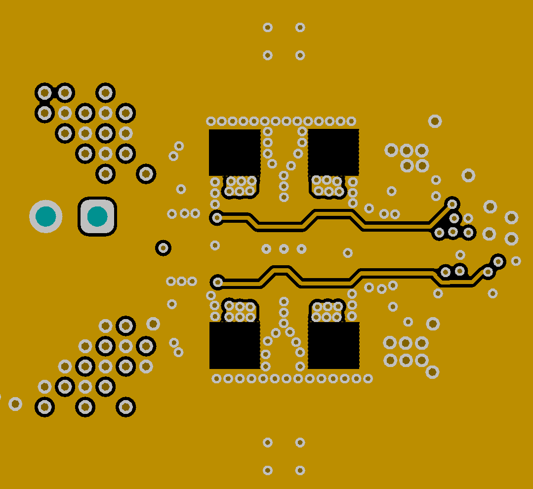
Board stack-up is shown in Figure 6-1. Figure 6-2 shows the top view of the entire board and Figure 6-3 through Figure 6-8 show the component placement, layout, and 3D view close to the LP875761-Q1 device.

GUID-B1F91A1C-9F4C-46DC-98B0-8CBB9BD21C8C-low.pngFigure 6-1 Board Stack-Up

The design utilizes dual side placement of the components. This allows placement of the inductors next to the LP875761-Q1 device for reducing SW node area for improved efficiency and reduced EMI. SW nets have also snubber components to reduce SW pin spiking and EMI. The input capacitors can be placed very close to the LP875761-Q1 device, to bottom side, to keep parasitic inductances low, and there is also space for input filters for further EMI reduction.
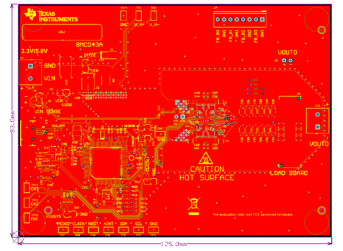
GUID-4DF76DF5-6F1B-4C52-8A96-51A1E6BD3EC2-low.pngFigure 6-2 Top View of the LP875761-Q1EVM
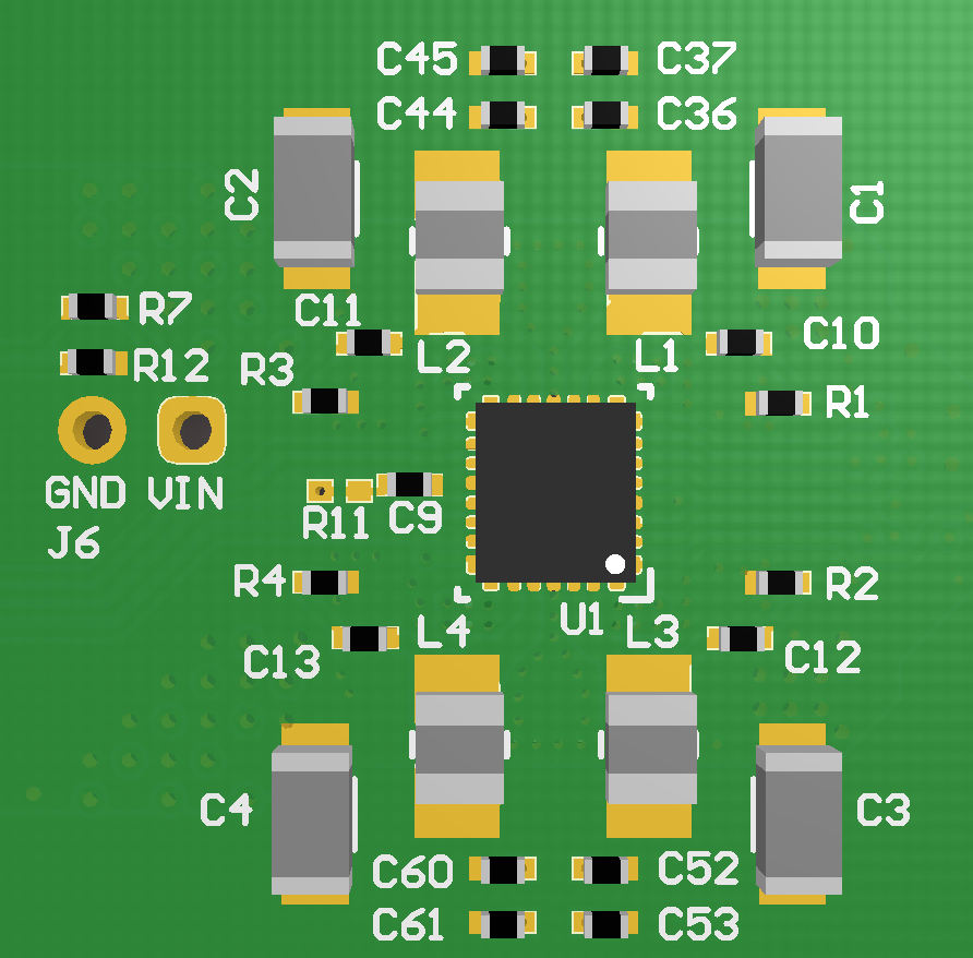
GUID-CB0441B1-6B90-4854-9513-D3DA41BD7863-low.pngFigure 6-3 Component Placement Top Layer
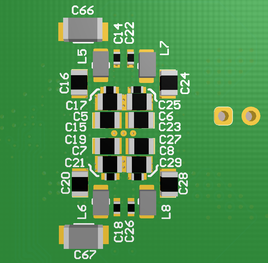
GUID-240A16D7-7BF4-43C1-A490-7C67E9FDBFDE-low.pngFigure 6-4 Component Placement Bottom Layer
GUID-D1D1EAD2-25BA-48EF-82CD-E32F904544A6-low.png
VIN nets are connected to bottom layer with multiple vias. This allows closer placement of the inductors, thus reducing SW node size and EMI. Also snubber circuits are placed next to SW nets for EMI reduction. Multiple GND vias are used to provide solid ground around the LP875761-Q1 device.
Figure 6-5 Top Layer
GUID-A73BD1DB-AC51-4B2F-92D2-9105D734B4BD-low.png
GND plane close to top layer (0.143 mm) helps to reduce parasitic inductance. Holes in the plane are under inductor footprint (SW node) to reduce parasitic capacitance of the SW node, thus reducing noise coupling and improving efficiency.
Figure 6-6 Mid-Layer1
GUID-416BB6D2-0BC4-49CC-BE6C-9B89CD402A7E-low.png
VIN supply is routed in this layer between the ground planes to reduce radiated emissions. VIN and GND vias are placed in hatched pattern to avoid large gaps in these planes.
Figure 6-7 Mid-Layer2
GUID-B2C3B67F-866B-47AE-BED1-62A066CA67F3-low.png
Input capacitors and filters are placed under the LP875761-Q1 into bottom layer. This allows closer placement of the inductors and input components reducing SW and VIN net areas and improving EMI.
Figure 6-8 Bottom Layer (note mirror view)