SPRAA99C March 2008 – May 2021 AM3351 , AM3352 , AM3354 , AM3356 , AM3357 , AM3358 , AM3359 , AM4372 , AM4376 , AM4377 , AM4378 , AM4379 , OMAPL138B-EP , TMUX646
4.3 Solder Ball Collapse
To produce the optimum solder joint, it is important to understand the amount of collapse of the solder balls, and the overall shape of the joint. These are a function of:
- The diameter of the package solder ball via.
- The volume and type of paste screened onto the PCB.
- The diameter of the PCB land.
- The board assembly reflow conditions.
- The weight of the package.
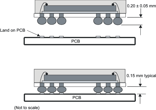
The original ball height on the package for a typical 0.5-mm-pitch package is 0.20 mm. After the package is mounted, this typically drops to 0.15 mm, as illustrated in Figure 4-1.
 Figure 4-1 Solder Ball Collapse
Controlling the collapse, and thus defining the package standoff, is critical to obtaining the optimum joint reliability. Generally, a larger standoff gives better solder joint fatigue strength, but this should not be achieved by reducing the board land diameter. Reducing the land diameter will increase the standoff, but will also reduce the minimum cross-section area of the joint. This, in turn, will increase the maximum shear force at the PCB side of the solder joint. Therefore, a reduction of land diameter will normally result in a worse fatigue life, and should be avoided unless all the consequences are well understood.