SPRABI1D January 2018 – July 2022 66AK2E05 , 66AK2G12 , 66AK2H06 , 66AK2H12 , 66AK2H14 , 66AK2L06 , AM5K2E02 , AM5K2E04 , SM320C6678-HIREL , TMS320C6652 , TMS320C6654 , TMS320C6655 , TMS320C6657 , TMS320C6670 , TMS320C6671 , TMS320C6672 , TMS320C6674 , TMS320C6678
- Trademarks
- 1 Introduction
- 2 Background
- 3 Migrating Designs From DDR2 to DDR3 (Features and Comparisons)
- 4 Prerequisites
- 5 Package Selection
-
6 Physical Design and Implementation
- 6.1 Electrical Connections
- 6.2 Signal Terminations
- 6.3
Mechanical Layout and Routing Considerations
- 6.3.1
Routing Considerations – SDRAMs
- 6.3.1.1 Mechanical Layout – SDRAMs
- 6.3.1.2 Stack Up – SDRAMs
- 6.3.1.3 Routing Rules – General Overview (SDRAMs)
- 6.3.1.4 Routing Rules – Address and Command Lines (SDRAMs)
- 6.3.1.5 Routing Rules – Control Lines (SDRAMs)
- 6.3.1.6 Routing Rules – Data Lines (SDRAMs)
- 6.3.1.7 Routing Rules – Clock Lines (SDRAMs)
- 6.3.1.8 Routing Rules – Power (SDRAMs)
- 6.3.1.9 Write Leveling Limit Impact on Routing – KeyStone I
- 6.3.1.10 Round-Trip Delay Impact on Routing – KeyStone I
- 6.3.1.11 Write Leveling Limit Impact on Routing – KeyStone II
- 6.3.1.12 Round-Trip Delay Impact on Routing – KeyStone II
- 6.3.2
Routing Considerations – UDIMMs
- 6.3.2.1 Mechanical Layout – UDIMMs
- 6.3.2.2 Stack Up – UDIMMs
- 6.3.2.3 Routing Rules – General Overview (UDIMMs)
- 6.3.2.4 Routing Rules – Address and Command Lines (UDIMMs)
- 6.3.2.5 Routing Rules – Control Lines (UDIMMs)
- 6.3.2.6 Routing Rules – Data Lines (UDIMMs)
- 6.3.2.7 Routing Rules – Clock Lines (UDIMMs)
- 6.3.2.8 Routing Rules – Power (UDIMMs)
- 6.3.2.9 Write-Leveling Limit Impact on Routing
- 6.3.1
Routing Considerations – SDRAMs
- 6.4 Timing Considerations
- 6.5 Impedance Considerations
- 6.6 Switching and Output Considerations
- 7 Simulation and Modeling
- 8 Power
- 9 Disclaimers
- 10References
- 11Revision History
6.5.2.1 Data Group Signals
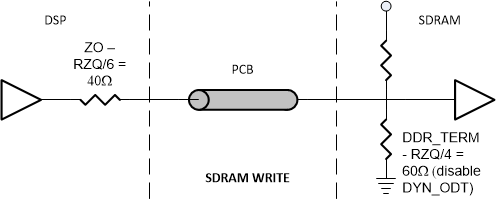
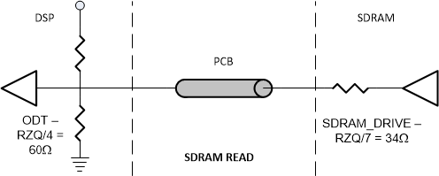
All data-group signals are point-to-point in the validated topologies. The data-group signals are driven by the KeyStone device on writes and driven by the SDRAM memories during reads. No external resistors are needed on these routes. The receivers in both cases (SDRAMs on writes and KeyStone device on reads) will assert on-die terminations (ODT) at the appropriate times. The following diagrams show the impedances seen on these nets during write and read cycles.
Figure 6-8 shows the impedances seen on the nets during a write cycle. During writes, the output impedance of the KeyStone II device is approximately 40 Ω. It is recommended that the SDRAM be implemented with a 240 Ω RZQ resistor and be configured to present an ODT of RZQ/4 for an effective termination of 60 Ω.
 Figure 6-8 Data Group Impedances During
Write Cycles on KeyStone II
Figure 6-8 Data Group Impedances During
Write Cycles on KeyStone IIFigure 6-9 shows the impedances seen on the nets during a read cycle. During reads, it is recommended that the SDRAM be configured for an effective drive impedance of RZQ/7 or 34 Ω (assuming RZQ resistor is 240 Ω). The ODT within the KeyStone II device will have an effective Thevenin impedance of 60 Ω.
 Figure 6-9 Data Group Impedances During
Read Cycles on KeyStone II