SPRAC21A June   2016  – June 2019 OMAP-L132 , OMAP-L138 , TDA2E , TDA2EG-17 , TDA2HF , TDA2HG , TDA2HV , TDA2LF , TDA2P-ABZ , TDA2P-ACD , TDA2SA , TDA2SG , TDA2SX , TDA3LA , TDA3LX , TDA3MA , TDA3MD , TDA3MV


  1.   TDA2xx and TDA2ex Performance
    1.     Trademarks
    2. SoC Overview
      1. 1.1 Introduction
      2. 1.2 Acronyms and Definitions
      3. 1.3 TDA2xx and TDA2ex System Interconnect
      4. 1.4 Traffic Regulation Within the Interconnect
        1. 1.4.1 Bandwidth Regulators
        2. 1.4.2 Bandwidth Limiters
        3. 1.4.3 Initiator Priority
      5. 1.5 TDA2xx and TDA2ex Memory Subsystem
        1. 1.5.1 Controller/PHY Timing Parameters
        2. 1.5.2 Class of Service
        3. 1.5.3 Prioritization Between DMM/SYS PORT or MPU Port to EMIF
      6. 1.6 TDA2xx and TDA2ex Measurement Operating Frequencies
      7. 1.7 System Instrumentation and Measurement Methodology
        1. 1.7.1 GP Timers
        2. 1.7.2 L3 Statistic Collectors
    3. Cortex-A15
      1. 2.1 Level1 and Level2 Cache
      2. 2.2 MMU
      3. 2.3 Performance Control Mechanisms
        1. 2.3.1 Cortex-A15 Knobs
        2. 2.3.2 MMU Page Table Knobs
      4. 2.4 Cortex-A15 CPU Read and Write Performance
        1. 2.4.1 Cortex-A15 Functions
        2. 2.4.2 Setup Limitations
        3. 2.4.3 System Performance
          1. 2.4.3.1 Cortex-A15 Stand-Alone Memory Read, Write, Copy
          2. 2.4.3.2 Results
    4. System Enhanced Direct Memory Access (System EDMA)
      1. 3.1 System EDMA Performance
        1. 3.1.1 System EDMA Read and Write
        2. 3.1.2 System EDMA Results
      2. 3.2 System EDMA Observations
    5. DSP Subsystem EDMA
      1. 4.1 DSP Subsystem EDMA Performance
        1. 4.1.1 DSP Subsystem EDMA Read and Write
        2. 4.1.2 DSP Subsystem EDMA Results
      2. 4.2 DSP Subsystem EDMA Observations
    6. Embedded Vision Engine (EVE) Subsystem EDMA
      1. 5.1 EVE EDMA Performance
        1. 5.1.1 EVE EDMA Read and Write
        2. 5.1.2 EVE EDMA Results
      2. 5.2 EVE EDMA Observations
    7. DSP CPU
      1. 6.1 DSP CPU Performance
        1. 6.1.1 DSP CPU Read and Write
        2. 6.1.2 Code Setup
          1. 6.1.2.1 Pipeline Copy
          2. 6.1.2.2 Pipeline Read
          3. 6.1.2.3 Pipeline Write
          4. 6.1.2.4 L2 Stride-Jmp Copy
          5. 6.1.2.5 L2 Stride-Jmp Read
          6. 6.1.2.6 L2 Stride-Jmp Write
      2. 6.2 DSP CPU Observations
      3. 6.3 Summary
    8. Cortex-M4 (IPU)
      1. 7.1 Cortex-M4 CPU Performance
        1. 7.1.1 Cortex-M4 CPU Read and Write
        2. 7.1.2 Code Setup
        3. 7.1.3 Cortex-M4 Functions
        4. 7.1.4 Setup Limitations
      2. 7.2 Cortex-M4 CPU Observations
        1. 7.2.1 Cache Disable
        2. 7.2.2 Cache Enable
      3. 7.3 Summary
    9. USB IP
      1. 8.1 Overview
      2. 8.2 USB IP Performance
        1. 8.2.1 Test Setup
        2. 8.2.2 Results and Observations
        3. 8.2.3 Summary
    10. PCIe IP
      1. 9.1 Overview
      2. 9.2 PCIe IP Performance
        1. 9.2.1 Test Setup
        2. 9.2.2 Results and Observations
    11. 10 IVA-HD IP
      1. 10.1 Overview
      2. 10.2 H.264 Decoder
        1. 10.2.1 Description
        2. 10.2.2 Test Setup
        3. 10.2.3 Test Results
      3. 10.3 MJPEG Decoder
        1. 10.3.1 Description
        2. 10.3.2 Test Setup
        3. 10.3.3 Test Results
    12. 11 MMC IP
      1. 11.1 MMC Read and Write Performance
        1. 11.1.1 Test Description
        2. 11.1.2 Test Results
      2. 11.2 Summary
    13. 12 SATA IP
      1. 12.1 SATA Read and Write Performance
        1. 12.1.1 Test Setup
        2. 12.1.2 Observations
          1. 12.1.2.1 RAW Performance
          2. 12.1.2.2 SDK Performance
      2. 12.2 Summary
    14. 13 GMAC IP
      1. 13.1 GMAC Receive/Transmit Performance
        1. 13.1.1 Test Setup
        2. 13.1.2 Test Description
          1. 13.1.2.1 CPPI Buffer Descriptors
        3. 13.1.3 Test Results
          1. 13.1.3.1 Receive/Transmit Mode (see )
          2. 13.1.3.2 Receive Only Mode (see )
          3. 13.1.3.3 Transmit Only Mode (see )
      2. 13.2 Summary
    15. 14 GPMC IP
      1. 14.1 GPMC Read and Write Performance
        1. 14.1.1 Test Setup
          1. 14.1.1.1 NAND Flash
          2. 14.1.1.2 NOR Flash
        2. 14.1.2 Test Description
          1. 14.1.2.1 Asynchronous NAND Flash Read/Write Using CPU Prefetch Mode
          2. 14.1.2.2 Asynchronous NOR Flash Single Read
          3. 14.1.2.3 Asynchronous NOR Flash Page Read
          4. 14.1.2.4 Asynchronous NOR Flash Single Write
        3. 14.1.3 Test Results
      2. 14.2 Summary
    16. 15 QSPI IP
      1. 15.1 QSPI Read and Write Performance
        1. 15.1.1 Test Setup
        2. 15.1.2 Test Results
        3. 15.1.3 Analysis
          1. 15.1.3.1 Theoretical Calculations
          2. 15.1.3.2 % Efficiency
      2. 15.2 QSPI XIP Code Execution Performance
      3. 15.3 Summary
    17. 16 Standard Benchmarks
      1. 16.1 Dhrystone
        1. 16.1.1 Cortex-A15 Tests and Results
        2. 16.1.2 Cortex-M4 Tests and Results
      2. 16.2 LMbench
        1. 16.2.1 LMbench Bandwidth
          1. 16.2.1.1 TDA2xx and TDA2ex Cortex-A15 LMbench Bandwidth Results
          2. 16.2.1.2 TDA2xx and TDA2ex Cortex-M4 LMBench Bandwidth Results
          3. 16.2.1.3 Analysis
        2. 16.2.2 LMbench Latency
          1. 16.2.2.1 TDA2xx and TDA2ex Cortex-A15 LMbench Latency Results
          2. 16.2.2.2 TDA2xx and TDA2ex Cortex-M4 LMbench Latency Results
          3. 16.2.2.3 Analysis
      3. 16.3 STREAM
        1. 16.3.1 TDA2xx and TDA2ex Cortex-A15 STREAM Benchmark Results
        2. 16.3.2 TDA2xx and TDA2ex Cortex-M4 STREAM Benchmark Results
    18. 17 Error Checking and Correction (ECC)
      1. 17.1 OCMC ECC Programming
      2. 17.2 EMIF ECC Programming
      3. 17.3 EMIF ECC Programming to Starterware Code Mapping
      4. 17.4 Careabouts of Using EMIF ECC
        1. 17.4.1 Restrictions Due to Non-Availability of Read Modify Write ECC Support in EMIF
          1. 17.4.1.1 Un-Cached CPU Access of EMIF
          2. 17.4.1.2 Cached CPU Access of EMIF
          3. 17.4.1.3 Non CPU Access of EMIF Memory
          4. 17.4.1.4 Debugger Access of EMIF via the Memory Browser/Watch Window
          5. 17.4.1.5 Software Breakpoints While Debugging
        2. 17.4.2 Compiler Optimization
        3. 17.4.3 Restrictions Due to i882 Errata
        4. 17.4.4 How to Find Who Caused the Unaligned Quanta Writes After the Interrupt
      5. 17.5 Impact of ECC on Performance
    19. 18 DDR3 Interleaved vs Non-Interleaved
      1. 18.1 Interleaved versus Non-Interleaved Setup
      2. 18.2 Impact of Interleaved vs Non-Interleaved DDR3 for a Single Initiator
      3. 18.3 Impact of Interleaved vs Non-Interleaved DDR3 for Multiple Initiators
    20. 19 DDR3 vs DDR2 Performance
      1. 19.1 Impact of DDR2 vs DDR3 for a Single Initiator
      2. 19.2 Impact of DDR2 vs DDR3 for Multiple Initiators
    21. 20 Boot Time Profile
      1. 20.1 ROM Boot Time Profile
      2. 20.2 System Boot Time Profile
    22. 21 L3 Statistics Collector Programming Model
    23. 22 Reference
  2.   Revision History

GP Timers

The GP Timers are good tools to have a quick measurement of performance of different initiators in the system. Though this provides a quick way to measure throughput, it should be kept in mind that there are some inherent errors involved with this technique of measurement. To make sure the measurement error is relatively small the transfer size should be kept larger. The typical pseudo code for the GP Timer-based throughput measurement is as follows:

/*Get the Timer Start Stamp*/ timerStartStamp = timerRead(TIMER_NUM); /*Start the transfer*/ transferStart(); /*Wait for Transfer Completion*/ waitForTransferCompletion(); /*Get the Time Stamp*/ timerEndStamp = timerRead(TIMER_NUM); /* Calculate the bandwidth - Note that one needs to multiply x2 from the calculated value to get * Bandwidth when the source and destination memory are the same */ if (timerEndStamp > timerStartStamp) BW = (((float) (TRANSFER_SIZE)/ (float) (timerEndStamp - timerStartStamp)) * TIMER_FREQ); else BW = (((float) (TRANSFER_SIZE)/ (float) (timerEndStamp - timerStartStamp + 0xFFFFFFFF)) * TIMER_FREQ);

The formulas used for the throughput calculations are:

Actual Throughput = (Transfer Size/Time Taken)

Ideal Throughput = Frequency of Limiting Port × Data Bus Width in Bytes

Utilization or Efficiency = (Actual Throughput/Ideal Throughput) × 100

Consider the data is transferred from one memory M1 to another memory M2.

The interconnect signals that implement OCP protocol used to transfer the data between the two memories, are as shown in Figure 7.
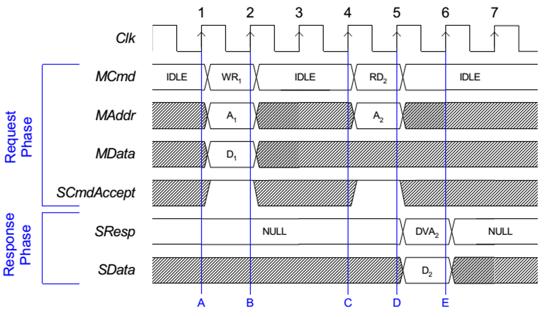
ocp_interconnect_signals_sprac21.pngFigure 7. OCP Interconnect Signals

There are two data lanes:

  • MData that contains the data to be written
  • SData that contains the data to be read

For further details on the exact operation of the OCP signals, see the OCP specifications.

Due to the presence of two data lanes, the case when the theoretical maximum throughput is obtained is when the MData contains valid data to be written and SData contains valid data to be read on every clock cycle of the transaction.

Mathematically stating this:

if Source Mem = Destination Mem, Ideal Throughputmem2mem = 2 × Frequency × Bus Width

if Source Mem ≠ Destination Mem, Ideal Throughputmem2mem = Frequency × Bus Width

Hence, when the source and destination memories are the same, the measured bandwidth should be multiplied into 2.