SPRAC21A June   2016  – June 2019 OMAP-L132 , OMAP-L138 , TDA2E , TDA2EG-17 , TDA2HF , TDA2HG , TDA2HV , TDA2LF , TDA2P-ABZ , TDA2P-ACD , TDA2SA , TDA2SG , TDA2SX , TDA3LA , TDA3LX , TDA3MA , TDA3MD , TDA3MV


  1.   TDA2xx and TDA2ex Performance
    1.     Trademarks
    2. SoC Overview
      1. 1.1 Introduction
      2. 1.2 Acronyms and Definitions
      3. 1.3 TDA2xx and TDA2ex System Interconnect
      4. 1.4 Traffic Regulation Within the Interconnect
        1. 1.4.1 Bandwidth Regulators
        2. 1.4.2 Bandwidth Limiters
        3. 1.4.3 Initiator Priority
      5. 1.5 TDA2xx and TDA2ex Memory Subsystem
        1. 1.5.1 Controller/PHY Timing Parameters
        2. 1.5.2 Class of Service
        3. 1.5.3 Prioritization Between DMM/SYS PORT or MPU Port to EMIF
      6. 1.6 TDA2xx and TDA2ex Measurement Operating Frequencies
      7. 1.7 System Instrumentation and Measurement Methodology
        1. 1.7.1 GP Timers
        2. 1.7.2 L3 Statistic Collectors
    3. Cortex-A15
      1. 2.1 Level1 and Level2 Cache
      2. 2.2 MMU
      3. 2.3 Performance Control Mechanisms
        1. 2.3.1 Cortex-A15 Knobs
        2. 2.3.2 MMU Page Table Knobs
      4. 2.4 Cortex-A15 CPU Read and Write Performance
        1. 2.4.1 Cortex-A15 Functions
        2. 2.4.2 Setup Limitations
        3. 2.4.3 System Performance
          1. 2.4.3.1 Cortex-A15 Stand-Alone Memory Read, Write, Copy
          2. 2.4.3.2 Results
    4. System Enhanced Direct Memory Access (System EDMA)
      1. 3.1 System EDMA Performance
        1. 3.1.1 System EDMA Read and Write
        2. 3.1.2 System EDMA Results
      2. 3.2 System EDMA Observations
    5. DSP Subsystem EDMA
      1. 4.1 DSP Subsystem EDMA Performance
        1. 4.1.1 DSP Subsystem EDMA Read and Write
        2. 4.1.2 DSP Subsystem EDMA Results
      2. 4.2 DSP Subsystem EDMA Observations
    6. Embedded Vision Engine (EVE) Subsystem EDMA
      1. 5.1 EVE EDMA Performance
        1. 5.1.1 EVE EDMA Read and Write
        2. 5.1.2 EVE EDMA Results
      2. 5.2 EVE EDMA Observations
    7. DSP CPU
      1. 6.1 DSP CPU Performance
        1. 6.1.1 DSP CPU Read and Write
        2. 6.1.2 Code Setup
          1. 6.1.2.1 Pipeline Copy
          2. 6.1.2.2 Pipeline Read
          3. 6.1.2.3 Pipeline Write
          4. 6.1.2.4 L2 Stride-Jmp Copy
          5. 6.1.2.5 L2 Stride-Jmp Read
          6. 6.1.2.6 L2 Stride-Jmp Write
      2. 6.2 DSP CPU Observations
      3. 6.3 Summary
    8. Cortex-M4 (IPU)
      1. 7.1 Cortex-M4 CPU Performance
        1. 7.1.1 Cortex-M4 CPU Read and Write
        2. 7.1.2 Code Setup
        3. 7.1.3 Cortex-M4 Functions
        4. 7.1.4 Setup Limitations
      2. 7.2 Cortex-M4 CPU Observations
        1. 7.2.1 Cache Disable
        2. 7.2.2 Cache Enable
      3. 7.3 Summary
    9. USB IP
      1. 8.1 Overview
      2. 8.2 USB IP Performance
        1. 8.2.1 Test Setup
        2. 8.2.2 Results and Observations
        3. 8.2.3 Summary
    10. PCIe IP
      1. 9.1 Overview
      2. 9.2 PCIe IP Performance
        1. 9.2.1 Test Setup
        2. 9.2.2 Results and Observations
    11. 10 IVA-HD IP
      1. 10.1 Overview
      2. 10.2 H.264 Decoder
        1. 10.2.1 Description
        2. 10.2.2 Test Setup
        3. 10.2.3 Test Results
      3. 10.3 MJPEG Decoder
        1. 10.3.1 Description
        2. 10.3.2 Test Setup
        3. 10.3.3 Test Results
    12. 11 MMC IP
      1. 11.1 MMC Read and Write Performance
        1. 11.1.1 Test Description
        2. 11.1.2 Test Results
      2. 11.2 Summary
    13. 12 SATA IP
      1. 12.1 SATA Read and Write Performance
        1. 12.1.1 Test Setup
        2. 12.1.2 Observations
          1. 12.1.2.1 RAW Performance
          2. 12.1.2.2 SDK Performance
      2. 12.2 Summary
    14. 13 GMAC IP
      1. 13.1 GMAC Receive/Transmit Performance
        1. 13.1.1 Test Setup
        2. 13.1.2 Test Description
          1. 13.1.2.1 CPPI Buffer Descriptors
        3. 13.1.3 Test Results
          1. 13.1.3.1 Receive/Transmit Mode (see )
          2. 13.1.3.2 Receive Only Mode (see )
          3. 13.1.3.3 Transmit Only Mode (see )
      2. 13.2 Summary
    15. 14 GPMC IP
      1. 14.1 GPMC Read and Write Performance
        1. 14.1.1 Test Setup
          1. 14.1.1.1 NAND Flash
          2. 14.1.1.2 NOR Flash
        2. 14.1.2 Test Description
          1. 14.1.2.1 Asynchronous NAND Flash Read/Write Using CPU Prefetch Mode
          2. 14.1.2.2 Asynchronous NOR Flash Single Read
          3. 14.1.2.3 Asynchronous NOR Flash Page Read
          4. 14.1.2.4 Asynchronous NOR Flash Single Write
        3. 14.1.3 Test Results
      2. 14.2 Summary
    16. 15 QSPI IP
      1. 15.1 QSPI Read and Write Performance
        1. 15.1.1 Test Setup
        2. 15.1.2 Test Results
        3. 15.1.3 Analysis
          1. 15.1.3.1 Theoretical Calculations
          2. 15.1.3.2 % Efficiency
      2. 15.2 QSPI XIP Code Execution Performance
      3. 15.3 Summary
    17. 16 Standard Benchmarks
      1. 16.1 Dhrystone
        1. 16.1.1 Cortex-A15 Tests and Results
        2. 16.1.2 Cortex-M4 Tests and Results
      2. 16.2 LMbench
        1. 16.2.1 LMbench Bandwidth
          1. 16.2.1.1 TDA2xx and TDA2ex Cortex-A15 LMbench Bandwidth Results
          2. 16.2.1.2 TDA2xx and TDA2ex Cortex-M4 LMBench Bandwidth Results
          3. 16.2.1.3 Analysis
        2. 16.2.2 LMbench Latency
          1. 16.2.2.1 TDA2xx and TDA2ex Cortex-A15 LMbench Latency Results
          2. 16.2.2.2 TDA2xx and TDA2ex Cortex-M4 LMbench Latency Results
          3. 16.2.2.3 Analysis
      3. 16.3 STREAM
        1. 16.3.1 TDA2xx and TDA2ex Cortex-A15 STREAM Benchmark Results
        2. 16.3.2 TDA2xx and TDA2ex Cortex-M4 STREAM Benchmark Results
    18. 17 Error Checking and Correction (ECC)
      1. 17.1 OCMC ECC Programming
      2. 17.2 EMIF ECC Programming
      3. 17.3 EMIF ECC Programming to Starterware Code Mapping
      4. 17.4 Careabouts of Using EMIF ECC
        1. 17.4.1 Restrictions Due to Non-Availability of Read Modify Write ECC Support in EMIF
          1. 17.4.1.1 Un-Cached CPU Access of EMIF
          2. 17.4.1.2 Cached CPU Access of EMIF
          3. 17.4.1.3 Non CPU Access of EMIF Memory
          4. 17.4.1.4 Debugger Access of EMIF via the Memory Browser/Watch Window
          5. 17.4.1.5 Software Breakpoints While Debugging
        2. 17.4.2 Compiler Optimization
        3. 17.4.3 Restrictions Due to i882 Errata
        4. 17.4.4 How to Find Who Caused the Unaligned Quanta Writes After the Interrupt
      5. 17.5 Impact of ECC on Performance
    19. 18 DDR3 Interleaved vs Non-Interleaved
      1. 18.1 Interleaved versus Non-Interleaved Setup
      2. 18.2 Impact of Interleaved vs Non-Interleaved DDR3 for a Single Initiator
      3. 18.3 Impact of Interleaved vs Non-Interleaved DDR3 for Multiple Initiators
    20. 19 DDR3 vs DDR2 Performance
      1. 19.1 Impact of DDR2 vs DDR3 for a Single Initiator
      2. 19.2 Impact of DDR2 vs DDR3 for Multiple Initiators
    21. 20 Boot Time Profile
      1. 20.1 ROM Boot Time Profile
      2. 20.2 System Boot Time Profile
    22. 21 L3 Statistics Collector Programming Model
    23. 22 Reference
  2.   Revision History

System Enhanced Direct Memory Access (System EDMA)

This section provides a throughput analysis of the EDMA module. The enhanced direct memory access module, also called EDMA, performs high-performance data transfers between two slave points, memories and peripheral devices without microprocessor unit (MPU) or digital signal processor (DSP) support during transfer. EDMA transfer is programmed through a logical EDMA channel, which allows the transfer to be optimally tailored to the requirements of the application. The EDMA can also perform transfers between external memories and between Device subsystems internal memories, with some performance loss caused by resource sharing between the read and write ports.

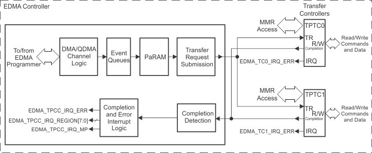
The EDMA controller block diagram is shown in Figure 10. The EDMA controller is based on two major principal blocks:

  • EDMA third-party channel controller (EDMA_TPCC)
  • EDMA third-party transfer controller (EDMA_TPTC)

The EDMA controller’s primary purpose is to service user programmed data transfers between internal or external memory-mapped slave endpoints. It can also be configured for servicing event driven peripherals (such as serial ports), as well. There are 64 direct memory access (DMA) channels and 8 QDMA channels serviced by two concurrent physical channels.
edma_controller_bd_sprac21.gifFigure 10. EDMA Controller Block Diagram

DMA channels are triggered by external event, manual write to event set register (ESR), or chained event. QDMA are auto-triggered when write is performed to the user-programmable trigger word. Once a trigger event is recognized, the event is queued in the programmed event queue. If two events are detected simultaneously, then the lowest-numbered channel has highest priority. Each event in the event queue is processed in the order it was queued. On reaching the head of the queue, the PaRAM associated with that event is read to determine the transfer details. The transfer request (TR) submission logic evaluates the validity of the TR and is submits a valid transfer request to the appropriate transfer controller. The maximum theoretical bandwidth for a given transfer can be found by multiplying the width of the interface and the frequency at which it transfers data.

The maximum speed the transfer can achieve is equal to the bandwidth of the limiting port. In general, a given transfer scenario will never achieve maximum theoretical band width due to several factors, like transfer overheads, access latency of source/destination memories, finite number of cycles taken by EDMA CC and EDMA TC between the time the transfer event is registered to the time the first read command is issued to EDMA TC. These overheads can be calibrated by looking at the time taken to do a 1 byte transfer. These factors are not excluded in these throughput measurements.

The frequency and bus widths of the different memory and slave end points are summarized in Table 8.

Table 8. Frequency and Bus Widths of Modules

Module Name Frequency (MHz) Bus Width (bits)
EDMA TPTC+TPTC 266 128
L3 266 128
OCMC RAM 266 128
EMIF 266 128
DSPL2 RAM 600 128
IVAHD SL2 388.33 128
ICSS RAM 200 32