SPRACK9 February 2019 AM1705 , AM1707 , AM1806 , AM1808 , OMAP-L132 , OMAP-L137 , OMAP-L138 , TMS320C6742 , TMS320C6745 , TMS320C6746 , TMS320C6747 , TMS320C6748
-
OMAP-L13x/C674x/AM1x schematic review guidelines
- Trademarks
- 1 Introduction
- 2 Recommendations Specific to OMAP-L1x/TMS320C674x/AM1x
- 3 BGA PCB Design
- 4 Power Management Solutions
- 5 References
- A XDS Connector Design Checklist
- B Connecting NOR Flash to OMAP-L138
2.3.4 Clocking
Make sure your input clock/crystal meets the data sheet requirements. For example:
- Frequency
- Voltage (if using external clock source)
- ESR for crystal
- Load capacitance meets both the crystal’s and processor’s requirements
- Crystal and caps placed physically close to processor
- Double check proper voltage level for clock (some devices will use core voltage, others I/O voltage).
- If there are any PLL configuration pins make sure they are set such that the resulting frequency is within device spec. Also, having alternate population options for those PLL pins could be handy.
OSC Internal Oscillator Clock Source
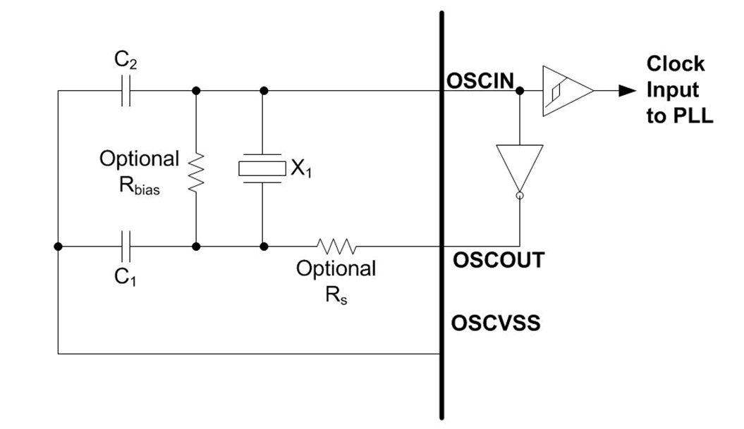
Figure 1 shows the recommended crystal circuit. It is recommended that pre-production printed circuit board (PCB) designs include the two optional resistors Rbias and Rs. They may be required for proper oscillator operation when combined with production crystal circuit components.
OSC Crystal Circuit Schematics
 Figure 1. Crystal Circuit
 In general, adding Rbias and Rs resistors improves circuit performance by reducing the long start-up time, crystal overdrive and voltage and temperature related issues. Specifically, they provide the following functionality:
- Rs helps reduce the drive level on the crystal and decreases the slew rate, which adds additional phase shift Recommended value: 50 Ω Rbias (a.k.a. the feedback resistor) is used to bias the input of the inverting amplifier and improve the loop gain Recommended value: 1M Ω
However, in most cases Rbias is not required and Rs is a 0-Ω resistor. These resistors may be removed from production PCB designs after evaluating oscillator performance with production crystal circuit components installed on pre-production PCBs.
For calculation of Rs and Rbias values, see www.crystek.com/documents/appnotes/Pierce-GateIntroduction.pdf.
Oscillator components (Crystal, C1, C2, optional Rbias and Rd) must be located close to the OMAPL1x package. Parasitic capacitance to the printed circuit board (PCB) ground and other signals should be minimized to reduce noise coupled into the oscillator.
Observation clock
CLKOUT is a PLL observation clock output, and is provided for test and debug purposes only. It should not be used as a synchronous clock for any of the peripheral interfaces because it was not timing-closed to any other signals. This clock output was not designed to drive any time-critical external circuits that require a low-jitter reference clock. There is no characterization data for the jitter performance for CLKOUT.