SPRACP5 December 2019 TMS320F2802-Q1 , TMS320F28020 , TMS320F280200 , TMS320F28021 , TMS320F28022 , TMS320F28022-Q1 , TMS320F280220 , TMS320F28023 , TMS320F28023-Q1 , TMS320F280230 , TMS320F28026 , TMS320F28026-Q1 , TMS320F28026F , TMS320F28027 , TMS320F28027-Q1 , TMS320F280270 , TMS320F28027F , TMS320F28027F-Q1 , TMS320F28030 , TMS320F28030-Q1 , TMS320F28031 , TMS320F28031-Q1 , TMS320F28032 , TMS320F28032-Q1 , TMS320F28033 , TMS320F28033-Q1 , TMS320F28034 , TMS320F28034-Q1 , TMS320F28035 , TMS320F28035-EP , TMS320F28035-Q1 , TMS320F28050 , TMS320F28051 , TMS320F28052 , TMS320F28052-Q1 , TMS320F28052F , TMS320F28052F-Q1 , TMS320F28052M , TMS320F28052M-Q1 , TMS320F28053 , TMS320F28054 , TMS320F28054-Q1 , TMS320F28054F , TMS320F28054F-Q1 , TMS320F28054M , TMS320F28054M-Q1 , TMS320F28055 , TMS320F2806-Q1 , TMS320F28062 , TMS320F28062-Q1 , TMS320F28062F , TMS320F28062F-Q1 , TMS320F28063 , TMS320F28064 , TMS320F28065 , TMS320F28066 , TMS320F28066-Q1 , TMS320F28067 , TMS320F28067-Q1 , TMS320F28068F , TMS320F28068M , TMS320F28069 , TMS320F28069-Q1 , TMS320F28069F , TMS320F28069F-Q1 , TMS320F28069M , TMS320F28069M-Q1
3 Gain Error
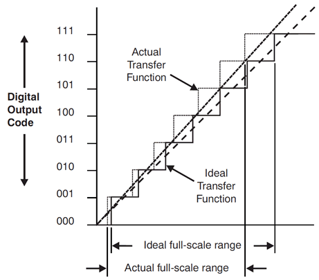
The gain error represents the deviation of the ADC’s actual transfer function to the ideal transfer function at the full scale range, maximum input voltage, after the offset error has been nullified. An ideal transfer function of an ADC is one in which the full scale range corresponds to the maximum output code. The F2803x devices have a 12 bit ADC with an internal reference of 3.3 V. For a resolution of 12 bits, the maximum digital output code is 4095. Therefore, in an ideal ADC, 3.3 V would map to a digital reading of 4095. The data sheet for this device family specifies that the gain error for the ADC is within ± 60 LSBs. Under these bounds, the ADC could interpret either 3.252 V (positive gain error) or a value up to 3.348 V (negative gain error) as the maximum output code reading instead of the full scale range. Positive gain error will saturate the converter at an earlier voltage reading; meaning all codes above a certain voltage threshold, depending on the amount of error, will result in the maximum output code.
NOTE
For the purpose of this analysis external reference mode was not considered.


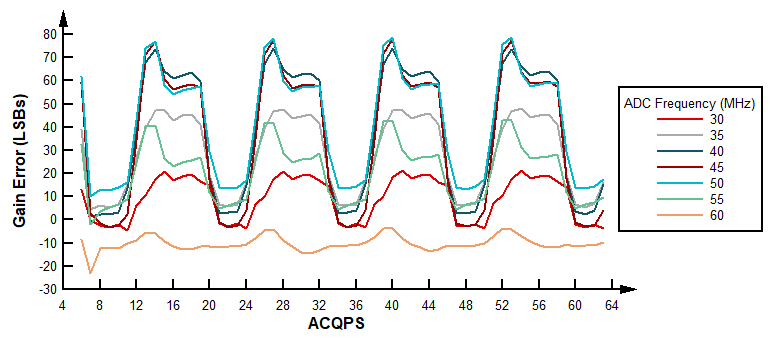
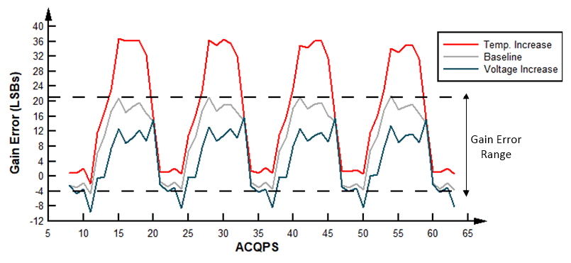
The gain error fluctuates in relation to ACQPS values when operating in overlap mode. Specifically referencing 30 and 60 MHz, as the operating temperature increases, the gain error range (maximum to minimum error value) also increases. 30 MHz is more susceptible to this change than 60 MHz. However, as temperature decreases, gain error becomes more dependent on the ADC operating frequency. This behavior causes some of the non-valid ACQPS values to have gain errors outside of the data sheet range.
An increase in voltage will shift the gain error down, towards larger negative values. This is however not applicable while operating at the lowest operable temperature because the error range does not shift with changes in VDDA.
Figure 6 shows these descriptions in a graphical form.

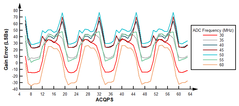
In non-overlap mode, input signals are only sampled while the ADC conversion stage is idle. Figure 7 illustrates how the gain error fluctuates in relation to ACQPS values when operating in non-overlap mode under nominal conditions. Much like overlap mode, the gain error range increases with increasing temperatures, solely in regards to 30 and 60 MHz; this shifted error range is still within the specified gain error range of ± 60 LSBs, as it is for all operable temperatures. Different values of VDDA will shift this range towards larger positive or negative gain errors depending on the operational frequency. For temperatures between the typical and maximum operable values, the larger VDDA voltages shift the gain error towards more negative values, as in overlap mode.

Based on the plots shown above, there are non-valid ACQPS values that have gain error that exceed those limits specified by the data sheet. In order to more closely model the ideal ADC transfer function, ACQPS values that have gain error outside of the data sheet specifications should be avoided as they can lead to an inaccurate representation of the full scale range.