SPRACY2 May 2021 TMUX646
1 Small Body nFBGA Package Details
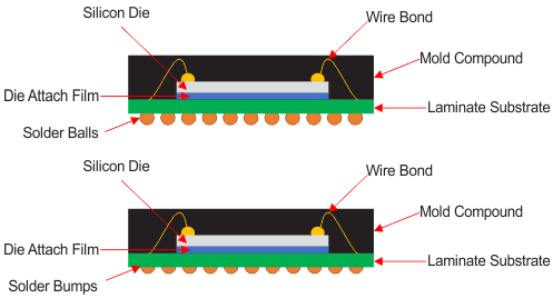
Figure 1-1 shows the structure of TI’s small body nFBGAs. Structure is nearly identical to that of the standard nFBGA shown in the Structure of TI's nFBGA Package image in nFBGA Packaging. The major difference is the package thickness. Standard nFBGAs have a thickness of ~1 mm while the small body variants can range from 0.45 mm - 1 mm. This is achieved by using a thinner substrate material and die attach film instead of epoxy.
Package stack up can be minimized even further by using solder bumps rather than the standard BGA solder balls. The reduced height of the bumps allows the smallest possible package height while offering exceptional board level reliability performance. The package seating height will be dependent upon the solder paste volume and land pad design. Table 1-1 lists all of TIs small body nFBGA packages.
 Figure 1-1 Structure of TI’s Small Body
nFBGAs
Figure 1-1 Structure of TI’s Small Body
nFBGAs| NMB | ZWA | NMN | NME | ZEC | |
|---|---|---|---|---|---|
| Total Number of Balls | 8 | 11 | 12 | 20 | 36 |
| *Length (L) (mm) | 2 | 2 | 2 | 2.5 | 2.45 |
| *Width (W) (mm) | 2 | 1.4 | 2.5 | 3 | 2.45 |
| Max Thickness (T) (mm) | 1.00 | 0.45 | 1.00 | 0.80 | 0.65 |
| Pitch (mm) | 0.5 | 0.5 | 0.5 | 0.5 | 0.4 |
| Ball Diameter (mm) | 0.30 | 0.25 | 0.30 | 0.30 | 0.25 |
| Total Balls in Width | 3 | 3 | 4 | 5 | 6 |
| Total Balls in Length | 3 | 4 | 3 | 4 | 6 |