SPRACY3 June 2021 F29H850TU , F29H859TU-Q1 , TMS320F280023C , TMS320F280025C , TMS320F280025C-Q1 , TMS320F280040C-Q1 , TMS320F280041C , TMS320F280041C-Q1 , TMS320F280048C-Q1 , TMS320F280049C , TMS320F280049C-Q1 , TMS320F28076 , TMS320F28379D , TMS320F28379D-Q1 , TMS320F28379S , TMS320F28386D , TMS320F28386D-Q1 , TMS320F28386S , TMS320F28386S-Q1 , TMS320F28388D , TMS320F28388S , TMS320F28P650DH , TMS320F28P650DK , TMS320F28P650SH , TMS320F28P650SK , TMS320F28P659DH-Q1 , TMS320F28P659DK-Q1 , TMS320F28P659SH-Q1
3.4 Completed Design
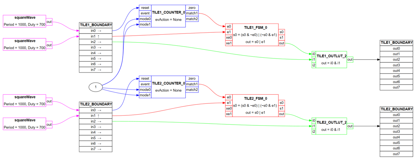
One of the tools provided with CCS is the graphical Tile Viewer showing all CLB components and the associated signal interconnections for a given CLB design. Figure 3-5 shows the completed block diagram of the design, including the logic connections among FSM, LUT and the Counter, with logic equations.
 Figure 3-5 Completed Design Block
Diagrams
Figure 3-5 Completed Design Block
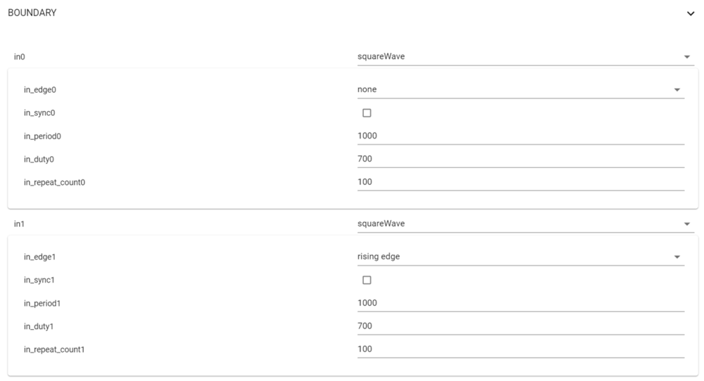
DiagramsIn addition, as shown in the block diagram, the “BOUNDARY” items are added as the tile inputs to simulate the CLB function before the test. As shown in Figure 3-5, both “in0” and “in1” are defined as a same periodic PWM referring to the trip signal, where the rising edge is selected for the “in-edge” option of “in1”. “in2” is set as 1, which represents normally high EPWM1B or EPWM2B.
 Figure 3-6 Boundary Input Setting
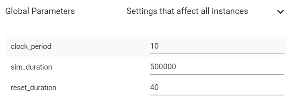
Once the CLB configuration and input stimuli have been defined, the simulation results can be obtained with the GTKwave viewer, as shown in Figure 3-7. And the expected delayed action is achieved at the CLB output signal. Note that the “clock_period” of the Global Parameters in the .syscfg tool should be changed to 10 ns, in order to match the time base of 100 MHz for CLB module, as shown in Figure 3-8. For more details of the CLB simulator, see the CLB Tool User's Guide.
 Figure 3-7 CLB Simulation Result
 Figure 3-8 Global Parameters
Configuration