SPRACY3 June 2021 F29H850TU , F29H859TU-Q1 , TMS320F280023C , TMS320F280025C , TMS320F280025C-Q1 , TMS320F280040C-Q1 , TMS320F280041C , TMS320F280041C-Q1 , TMS320F280048C-Q1 , TMS320F280049C , TMS320F280049C-Q1 , TMS320F28076 , TMS320F28379D , TMS320F28379D-Q1 , TMS320F28379S , TMS320F28386D , TMS320F28386D-Q1 , TMS320F28386S , TMS320F28386S-Q1 , TMS320F28388D , TMS320F28388S , TMS320F28P650DH , TMS320F28P650DK , TMS320F28P650SH , TMS320F28P650SK , TMS320F28P659DH-Q1 , TMS320F28P659DK-Q1 , TMS320F28P659SH-Q1
1 Introduction
Nowadays, three-level inverter topology has become increasingly popular in high power applications, like UPS and solar inverter. By increasing the bus voltage to 1000-V or 1500-V DC, the current can be reduced to maintain the same power levels, which can significantly reduce the power loss with less copper design. Besides, three-level inverter topology makes it possible to use the same switching device to support this much higher voltage stress than before. However, compared with traditional two-level inverter, in addition to more complicated power conversion control, a different fault protection scheme is required for three-level inverter.
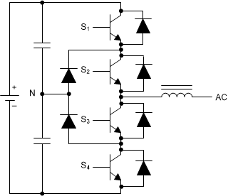
Figure 1-1 shows a typical single phase three-level I-Type inverter, named neutral point clamped (NPC) inverter. The single phase NPC inverter includes 4 FETs, like IGBT, in series, where S1 and S4 are called outer switches, with S2 and S3 called inner switches.
 Figure 1-1 Single Phase Three-Level I-Type
Inverter
Figure 1-1 Single Phase Three-Level I-Type
InverterThe based control of the four series FETs are as follows.
- S1 always switches opposite of S3, and S4 always switches opposite of S2. There is a dead time between S1 and S3, as well as between S4 and S2, which always prevents a shoot-through condition.
- S1 and S4 cannot be on simultaneously.
Considering the difference between positive cycle and negative cycle when tied to the grid, the general switching states of 4 FETs in normal operation are shown in Table 1-1.
| Symbol | Switching States | |||
|---|---|---|---|---|
| S1 | S2 | S3 | S4 | |
| Positive | Alternate switch | Remaining ON | Alternate switch | Remaining OFF |
| Negative | Remaining OFF | Alternate switch | Remaining ON | Alternate switch |
There are several events which lead to quick shut-down to protect the semiconductors and the system, like over current, thermal overload, and so forth. Unlike immediately switching off all the FETs simultaneously in two level inverter, for three-level inverter, it must be made sure that the correct switch-off sequence is maintained: outer switches (S1 or S4) off first, inner switches (S2 or S3) off after a specific delay, while the inner one must be switched on firstly during the recover process. This delayed protection requirement has been a challenge for lots of UPS or solar inverter customers for a long time. Since using software algorithm will cause too much delay to provide in-time protection, some customers have to use external hardware circuits, like FPGA or CPLD, to achieve such protection logic, which increases the system cost and also the development effort.
The C2000 configurable logic block (CLB) is a collection of configurable blocks that interconnect through software to implement custom digital logic functions, which can be an option to replace the function achieved by external CPLD or FPGA. This application report has designed and validated a simple protection scheme with CLB, and also discussed several extra requirements in three-level inverter. The example code is based on F280049C, and it can be easily migrated to any other C2000 devices with CLB, including F28388D/S, F28386D/S, F28379D/S, F28076 and F28004xC.